effect of Asz on the growth of AlGaAs is lx10l8, and 2x1018 cm
advertisement
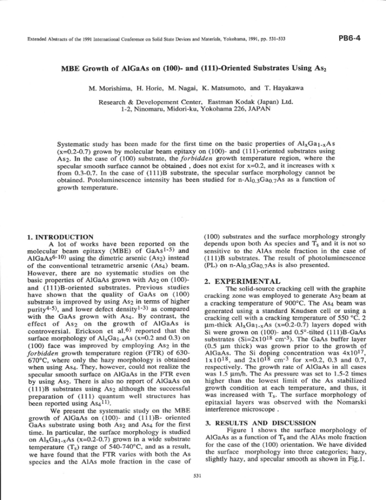
Extended Abstracts of the l99l International Conference on Solid State Devices and Materials, Yokohama, 1991, pp. 531-533 PB6-4 MBE Growth of AlGaAs on (100)- and (111)-Oriented Substrates Using As2 M. Morishima, H. Horie, M. Nagai, K. Matsumoto, and T. Hayakawa Research & Developement Center, Eastman Kodak (Japan) Ltd. 1-2, Ninomaru, Midori-ku, Yokohama226, JAPAN Systematic study has been made for the first time on the basic properties of Al*Ga1-1As (x=0.2-0.7) grown by molecular beam epitaxy on (100)- and (lll)-oriented substrates using AsZ. In the case of (100) substrate, the forbidder? growth temperature region, where the specular smooth surface cannot be obtained , does not exist for x=0.2, and it increases with x from 0.3-0.7. In the case of (l1l)B substrate, the specular surface morphology cannot be obtained. Potoluminescence intensity has been studied for n-Alg.3Gag.7As as a function of growth temperature. (100) substrates and the surface morphology strongly depends upon both As species and Tr and it is not so I.. INTRODUCTION A lot of works have been reported on the molecular beam epitaxy (MBE) of GaAsl-5) and sensitive to the AlAs mole fraction in the case of (111)B substrates. The result of photoluminescence (PL) on n-Als.3Gag.7As is also presented. AlGaAs6-10) using the dimetric arsenic (Asz) instead of the conventional tetrametric arsenic (As+) beam. However, there are no systematic studies on the basic properties of AlGaAs grown with As2 on (100)and (l I l)B-oriented substrates. Previous studies have shown that the quality of GaAs on ( 100) substrate is improved by using AsZ in terms of higher purity4-5), and lower defect densityl-3) as compared with the GaAs grown with As+. By contrast, the effect of Asz on the growth of AlGaAs is controversial. Erickson et al.6) reported that the surface morphology of Al"Ga1-1As (x=0.2 and 0.3) on (100) face was improved by employing As2 in the forbidden growth temperature region (FTR) of 630670oC, where only the hazy morphology is obtained 2. EXPERIMBNTAL The solid-source cracking cell with the graphite cracking zone was employed to generate Asz beam at a cracking temperature of 900"C. The As4 beam was generated using a standard Knudsen cell or using a cracking cell with a cracking temperature of 550 "C.2 pm-thick Al;Ga1-yAs (x=0.2-0.7) layers doped with Si were grown on (100)- and O.5o-tilted (1ll)B-GaAs substrates (Si=2x1018 cm-3;. The GaAs buffer layer (0.5 pm thick) was grown prior to the growth of AlGaAs. The Si doping concentration was 4x10¹⁷, lx10l8, and 2x1018 cm-3 for x=0.2, 0.3 and 0.7, respectively. The growth rate of AlGaAs in all cases was 1.5 pm/h. The As pressure was set to 1.5-2 times higher than the lowest limit of the As stabilized growth condition at each temperature, and thus, it was increased with Ts. The surface morphology of epitaxial layers was observed with the Nomarski when using As+. They, however, could not realize the specular smooth surface on AlGaAs in the FTR even by using Asz. There is also no report of AlGaAs on (lll)B substrates using As2 although the successful preparation -been of (11 1) quantum well structures has reported using As4ll;. We present the systematic study on the MBE growth of AlGaAs on (100)- and (lll)B- oriented GaAs substrate using both As2 and As4 for the first time. In particular, the surface morphology is studied on Al1Ga1-xAs (x=0.2-0.7) grown in a wide substrate temperature (Tr) range of 540-740oC, and as a result, we have found that the FTR varies with both the As species and the AlAs mole fraction in the case of interference microscope 3. RESULTS AND DISCUSSION Figure I shows the surface morphology of AlGaAs as a function of Tr and the AlAs mole fraction for the case of the (100) orientation. We have divided the surface morphology into three categories; hazy, slightly hazy, and specular smooth as shown in Fig.1. 531 O: specular smooth A: sfightly hazy \ : hazy 1.0 ;o 0.8 ? G 0.6 .,' o o'4 oc COCC Asa, smooth (pyramid-like) A: )(: slighily hazy hazy (111)8 (a) o E 0.6 IL ut o o o.4 o =q, OC o a faceted : z o c $o 0.2 x (a) lt =o specular f 1.0 Aso, (100) x O: s o.2 0.0 1.0 Asr, x ;o 0.8 ? E 0.6 5 o o.4 (100) 1.0 G) oo lt = 3 As2, (111)B x io o.a 3 E o.e ,t 0.4 (b) ll. ooco CCC oo 0-2 o = &, o.2 0.0 550 Fig.l 600 650 700 750 SUBSTRATE TEMPERATURE: Ts ("C) of Al*Gat-xAs as a of AlAs mole fraction and substrate Surface morphology function temperature grown with (a) As+ and (b) As2 in the case of (100) orientation. Shaded region correspond to the region where the specular smooth surface cannot be realized. The "hazy" surface can be recognized as hazy by the naked eyes. The "slightly hazy" surface appears to be smooth to the naked eyes, however, some undulation can be observed by using Nomarski microscope. The "specular smooth" surface shows no undulation even with the Nomarski microscope. When As4 is used, the FTR is in the range of 630-7l0oc, which does not depend upon the AlAs mole fraction [Fig.l(a)]. By contrast, when As2 is used, the FTR does not exist for x=0.2, otrd it varies from 550-610"C for x=0.3 to 550-710oC for x=0.7 [Fig.l(b)]. Moreover the low end of FTR shifts to lower temperature by about 80'C when As2 is used. These results cannot be explained by a simple model. It is important to note that the surface morphology is, at least, improved within the FTR and vanished FTR for x=0.2 by using Asz. This, however, dose not necessarily mean the enhancement of the specular smooth surface region. In Fig 2, surface morphology is shown for the (111)8 orientation. We add the one more category, "faceted" surface. The "faceted 3' surface exhibits well-known pyramid-likel2) rcxftred surface. The specular smooth surface cannot be obtained in the whole range of Ts when using Asz. This result 550 Fig.2 600 700 750 Ts ("C) of AlxG a 1-*As as a of AlAs mole fraction and substrate Surface morphology function temperature grown case 650 SUBSTRATE TEMPERATURE: of (111)8 with (a) Asa and (b) As2 in the orientation. Deeper shade region correspond to the region of the faceted (pyramid-like) morphology. indicates that the specular smooth surface obtained at high Ts using As4 does not result from the cracking of As4 at the growth surface. We have observed that the shape of some of surface defects in case of the As2 growth is different from that of As4 growth. Thus the growth kinetics is different depending on the As species. The dissociate reaction of As4 into As2 at the growth surface might play an important role for the of As+. The PL intensity has been measured at room temperature for Alg.3Gag.7As layers. As shown in Fig. 3, the PL intensity is lower for the layers grown with As2 than that for the layers grown with As4 in both cases of (100) and (1ll)B orientations. In the case of (111)B orientation [Fig 3.(b)], samples grown at low Ts ( 620-630 oC both with As2 and As4 show almost same PL intensity, which increases with Tr. In this T, region, the surface morphology shows the faceted morphology shown in Fig. 2. We have found a large density of microtwins and stacking faults in Alo.7Ga0.3As with faceted surface by TEM case observationsl3). These defects have never been found in the samples in the other categories. Therefore the 10 (100) o c .= (111)B o 3 o d cl o .= c F I ih z .d IJJ (E J = G F F ct 1L (a) Fig.3 500 z uJl 550 600 650 700 750 = J o suBsrRATE TEMPERATURE ("C) Room-temperature qhotoluminescence intensity of Alg.3Gag.7As (Si=101u cm-r) grown on (a) (100) and (b) (l1l)B orientation with As4 and As2 as a function of substrate temperature. (b) 500 550 600 650 700 ''B'TRATETEMPERAT'RE 750 fc) REFFERENCES 1) J.H.Neave, P.Blood, and B.A.Joyce: Appl. Phys. I-eu. g(1980)31 1. PL intensity in the low Tr range should be determined by the high density of crystallographic defects, such as microtwins and stacking faults. We consider that 2) H.Kiinzel, J.Knecht, H.Jung, K.Wunstel, these results are due to the stable As trimers structurel3-15) which hinders Ga incorporation into proper lattice sitesl3). On the other hand, the PL intensity strongly depend upon the degree of As stabilization in the high Ts range and it is determined by the density of point defects, such &s, As interstitials and antisite defects. In addition, the formation of the pyramid-like surface morphology is strongly related with the formation of stacking faults K.Ploog: Appl. Phys. A28(1982)167 and . 3) M.Missous and K.E.Singer: Appl. Phys. Lett. 50 (1987)694. 4) J.C.Garcia, A.C.Beye, J.P.Contour, G.Neu, and J.Massies: Appl. Phys. Lett. 5) 2(1988)1596. C.R.Stanley, MC.Holland, A.H.Kean, M.B. Stanaway, R.T.Grimes, and J.M.Chamberlain: Appl. Phys. Lett. 58(1991)478. 6) L.P.Erickson, T.J.Mattord, P.W.Palmberg, R.Fischer, and H.Morkog: Electron. Lett. and/or microtwins. l9(1983)633. 4. CONCLUSION 7) G.Duggan, P.Dawson, C.T.Foxon, and G.W.Fooft: J.Phys.(Paris), Colloq. &(1982)C5 -129 . 8) R.N.Sacks, D.W.Eichler, R.A.Pastrello, and We have grown AlGaAs on ( 100)- and (1ll)B-oriented GaAs substrates by MBE using As2 and As4. We have observed that FTR does not exist for x=0.2 and it increases with x from 0.3 to 0.7 in the case of (100) orientation. We cannot obtain the specular smooth surface in the whole range of Ts of 540-740"C of T5 in the case of (111)B orientation. This can be partly attributed to the shorter migration length of Al due to the higher reactivity of As2 than As+. The second order reaction process of As4 should play an important role for realizing good quality. The first order reaction process of As2 possibly required the tighter control of As pressure because the lack of the intermediate or associate reaction, and the second order reaction of As4 favorably act as on limiting process in the MBE growth of AlGaAs. P.Colombo, J. Vac. Sci. Technol. EE(1990)168. 9) J.Y.K., D.Bassi, and L.Jostad: Appl. Phys. Kett. 5Z(l 990)2107 . 10) J.Y.Kim, D.Bassis, J.Ellis, and L.Jostad: Appl. Phys. Lett. f,(1990)2333. 1 l) T.Hayakawa, T.Suyama, K.Takahashi, M.Kondo, S.Yamamoto, T.Hijikata:. Appl.Phys. Lett.52 (re88)33e. l2) K.Tsutsui, H.Mizukami,O.Ishiyama, S.Nakamura, and S.Furukawa: Jpn.J.Appl.Phys.29(1 990)468. 13) T.Hyakawa, M.Morishima, and S.Chen: 5th International Conference on Modulated Semiconductor Structeres , NaJa, July, PA-l8, 1991. 14) D.K.Biegelsen, R.D.Bringans: J.E.Northrup, and L.-E.Swarts. Phys. Rev. Lett. 65(1990)452. 15) P.Chewn, K.C.Rajkumar and A.Madhukar: Appl. Phys. Lett. 5E(199 l)177 l. ACKNOWLEDGEMENTS Authors would like to thank to S. Chen (Eastman Kodak Company) for TEM measurements and fruitful discussion. 533
