Preliminary Technical Data
400 MHz – 4 GHz Low Noise Amplifier
ADL5523
FEATURES
17.5 dB Gain at 1950MHz
Matched 50-Ω input and output
Noise Figure of1.0 dB 1950MHz
OIP3 of 33.7dBm typ at 1950MHz
Single 5V Supply Operation
Operating current of 65ma at +5V
LFCSP 3x3 mm Package
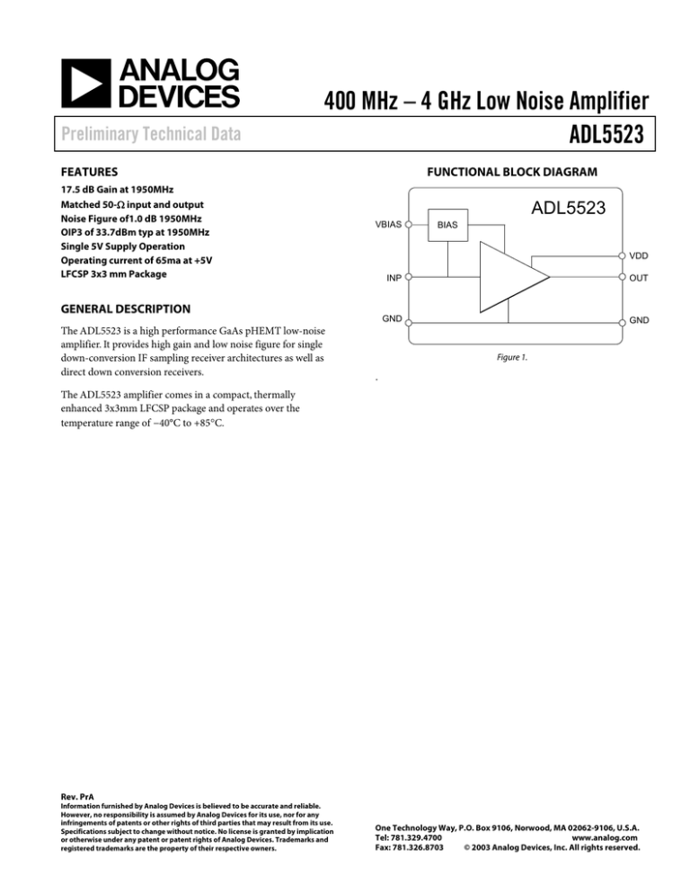
FUNCTIONAL BLOCK DIAGRAM
ADL5523
VBIAS
VDD
GENERAL DESCRIPTION
The ADL5523 is a high performance GaAs pHEMT low-noise
amplifier. It provides high gain and low noise figure for single
down-conversion IF sampling receiver architectures as well as
direct down conversion receivers.
BIAS
INP
OUT
GND
GND
Figure 1.
.
The ADL5523 amplifier comes in a compact, thermally
enhanced 3x3mm LFCSP package and operates over the
temperature range of −40°C to +85°C.
Rev. PrA
Information furnished by Analog Devices is believed to be accurate and reliable.
However, no responsibility is assumed by Analog Devices for its use, nor for any
infringements of patents or other rights of third parties that may result from its use.
Specifications subject to change without notice. No license is granted by implication
or otherwise under any patent or patent rights of Analog Devices. Trademarks and
registered trademarks are the property of their respective owners.
One Technology Way, P.O. Box 9106, Norwood, MA 02062-9106, U.S.A.
Tel: 781.329.4700
www.analog.com
Fax: 781.326.8703
© 2003 Analog Devices, Inc. All rights reserved.
Preliminary Technical Data
ADL5523
SPECIFICATIONS
VS = 5 V, T = 25°C, ZS = ZL = 50Ω , fC= 1950MHz
Table 1.
Parameter
Conditions
Min
Typ
Max
Unit
Input return loss
External match
14
dB
Output return loss
External match
13
dB
17.5
dB
Gain
Gain Flatness
In the [1920 – 1980] frequency band
0.015
dB/MHz
Gain Tempco
In the [1920 – 1980] frequency band
0.011
dB/°C
Noise Figure
1.0
dB
Output IP3
33.7
dBm
Output 1 dB Compression Point
21.9
dBm
S12 Isolation
22
dB
POWER-INTERFACE
Supply Voltage
4.5
Current Consumption
5
65
Rev. PrA | Page 2 of 6
5.5
V
mA
Preliminary Technical Data
ADL5523
ABSOLUTE MAXIMUM RATINGS
Table 2.
Parameter
Supply Voltage, VPOS
Max RF Input Level
Internal Power Dissipation
θJA (Exposed paddle soldered down)
θJA (Exposed paddle not soldered down)
θJC (At exposed paddle)
Maximum Junction Temperature
Operating Temperature Range
Storage Temperature Range
Lead Temperature Range
(Soldering 60 sec)
Rating
5.5 V
TBD
TBD mW
TBD mW
TBD°C/W
TBD°C/W
TBD°C/W
TBD°C
–40°C to +85°C
–65°C to +150°C
Stresses above those listed under Absolute Maximum
Ratings may cause permanent damage to the device.
This is a stress rating only; functional operation of the
device at these or any other conditions above those
listed in the operational sections of this specification
is not implied. Exposure to absolute maximum rating
conditions for extended periods may affect device
reliability.
ESD CAUTION
ESD (electrostatic discharge) sensitive device. Electrostatic charges as high as 4000 V readily accumulate on the
human body and test equipment and can discharge without detection. Although this product features
proprietary ESD protection circuitry, permanent damage may occur on devices subjected to high energy
electrostatic discharges. Therefore, proper ESD precautions are recommended to avoid performance
degradation or loss of functionality.
Rev. PrA | Page 3 of 6
Preliminary Technical Data
ADL5523
PIN CONFIGURATION AND FUNCTIONAL DESCRIPTIONS
1
VBIAS
2
INP
3
4
VDD 8
ADL5523 OUT
top view
NC
NC
(not to scale)
NC
Exposed pad
7
6
NC 5
Figure 2. 8-Lead LFCSP
Table 3. Pin Function Descriptions- 8 Lead CSP
Pin No.
1
2
3,4,5,6
7
8
Mnemonic
VBIAS
INP
NC
OUT
VDD
Exposed pad
EP
Description
Bias: Internal DC bias
RF Input: Must be AC-coupled.
NC: No internal connection
RF Output: Must be AC-coupled.
Supply: VDD bias needs to be bypassed to ground using
low-inductance capacitors.
Exposed Paddle: Connect to a low impedance ground plane
Rev. PrA | Page 4 of 6
Preliminary Technical Data
ADL5523
OIP3 - dBm
TYPICAL PERFORMANCE
CHARACTERISTICS
76
74
IPOS - mA
72
70
38
37
36
35
34
33
32
31
30
29
28
27
26
25
68
-40°C (1920MHz
1950MHz
1980MHz)
+25°C (1920MHz
1950MHz
1980MHz)
+85°C (1920MHz
1950MHz
1980MHz)
-8
-6
-4
-2
0
2
4
6
8
10
12
14
16
18
20
Pout - dBm
66
Figure 7.O IP3 vs. Output Power, Temperature and Frequency
64
62
-40
-30
-20
-10
0
10
20
30
40
50
60
70
80
90
Temperature - degC
1.4
1.2
Noise Figure - dB
Figure 3. ADL5523 Current vs. Temperature
25
Gain (-40°C
+25°C
+85°C)
15
0.6
0.4
10
0.2
Output Power (-40°C
+25°C
+85°C)
5
0
1920
1930
1940
1950
1960
1970
1980
Frequency - MHz
0
-5
-25
-20
-15
-10
-5
0
5
Figure 8.Distribution of Noise Figure for Five Parts, 1920 to 1980 MHz
10
Pin - dBm
5
Figure 4. Output Power and Gain vs. Temperature
4.5
4
OIP3 (-40°C
+25°C
+85°C)
Gain, P1dB - dB(m)
28
26
24
22
16
14
1920
30
25
P1dB (-40°C
+25°C
+85°C)
20
20
18
35
15
Gain (-40°C
+25°C
+85°C)
1930
Noise Figure - dB
40
OIP3 - dBm
30
3.5
3
2.5
2
1.5
1
0.5
0
400
10
900
1400
5
1940
1950
1960
1970
0
1980
Freq - MHz
1900
2400
2900
Frequency - MHz
Figure 9. Distribution of Noise Figure for Five Parts, Complete Frequency
Range
Figure 5. Gain, P1dB, OIP3 vs. Frequency
20
15
S21
10
20
5
S-parameters - dB
18
16
14
Gain (dB)
Pout (dBm), Gain (dB)
20
1
0.8
12
10
0
-5
S22
-10
-15
8
S11
-20
6
S12
-25
4
-30
2
0
400
1920
1930
1940
1950
1960
1970
Freq - MHz
900
1400
1900
2400
2900
Figure 10. Typical S Parameters, 1920 to 1980 MHz
Frequency - MHz
Figure 6. Gain vs. Frequency, Complete Frequency Range, 5 Parts
Rev. PrA | Page 5 of 6
1980
ADL5523
Preliminary Technical Data
OUTLINE DIMENSIONS
3.25
3.00 SQ
2.75
0.60 MAX
2.95
2.75 SQ
2.55
TOP
VIEW
PIN 1
INDICATOR
0.50
BSC
8
1.89
1.74
1.59
(BOTTOM VIEW)
0.70 MAX
0.65 TYP
5
PIN 1
INDICATOR
4
1.60
1.45
1.30
0.05 MAX
0.01 NOM
0.20 REF
022107-A
0.90 MAX
0.85 NOM
1
EXPOSED
PAD
0.30
0.23
0.18
12° MAX
0.50
0.40
0.30
Figure 3. 8-Lead Lead Frame Chip Scale Package [LFCSP_VD]
3mm × 3 mm Body, Very Thin, Dual Lead
CP-8-2
Dimensions shown in millimeters
ORDERING GUIDE
Model
ADL5523ACPZ-R71
ADL5523ACPZ-WP1
ADL5523-EVALZ
1
Temperature Range
– 40 ° C to + 8 5 ° C
–40°C to +85°C
Package Description
7 ” T a pe a n d R e e l
Waffle Pack
Ev aluation Boar d
Z = Pb free part
©2007 Analog Devices, Inc. All rights reserved. Trademarks and
registered trademarks are the property of their respective owners.
PR06829-0-5/07(PrA)
Rev. PrA | Page 6 of 6
Package Option
C P - 8- 2
CP-8-2
