Pass-Transistor
advertisement
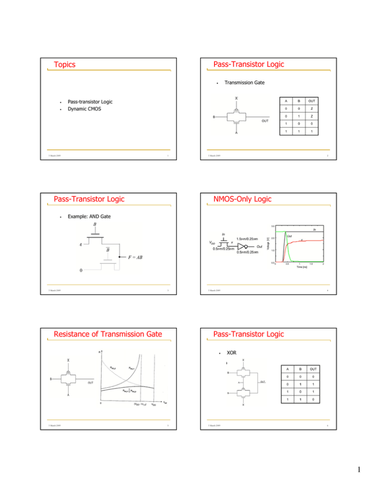
Pass-Transistor Logic Topics Transmission Gate • • • Pass-transistor Logic Dynamic CMOS 3 March 2009 1 Pass-Transistor Logic • 3 March 2009 NMOS-Only Logic Example: AND Gate 3 March 2009 3 Resistance of Transmission Gate 3 March 2009 4 Pass-Transistor Logic • 3 March 2009 2 5 3 March 2009 XOR 6 1 Pass-Transistor Logic • • • • • • Dynamic CMOS In static circuits at every point in time (except when switching) the output is connected to either GND or VDD via a low resistance path. • In many cases, uses fewer transistors Can be difficult to design Usually requires complemented versions of all signals Difficult to layout Transmission gate looks like a RC line Delay analysis is not as well defined in terms of sizing choices fan-in of n requires 2n transistors (n N-type and n P-type) Dynamic circuits rely on the temporary storage of signal values on the capacitance of high impedance nodes. • requires only n+2 (n+1 N-type and 1 P-type) transistors (can be further reduced to n+1) 3 March 2009 7 Dynamic CMOS • 3 March 2009 8 Dynamic Gate nMOS logic structure with pre-charged pullup •Pre-charge to VDD when clock is low •Evaluate when clock is high 3 March 2009 9 Conditions on Output • • • 3 March 2009 3 March 2009 10 Properties of Dynamic Gates Once the output of a dynamic gate is discharged, it cannot be charged again until the next pre-charge operation. Inputs to the gate can make at most one transition during evaluation. Output can be in the high impedance state during and after evaluation (PDN off), state is stored on CL • Logic function is implemented by the PDN only • • 11 3 March 2009 number of transistors is N + 2 (versus 2N for static complementary CMOS) Full swing outputs (VOL = GND and VOH = VDD) Sizing of the devices does not affect the logic levels (ratioless) 12 2 Properties of Dynamic Gates Properties of Dynamic Gates Faster switching speeds • 3 March 2009 13 Properties of Dynamic Gates 3 March 2009 14 Advantages • low noise margin (NML) Needs a pre-charge/evaluate clock • 15 Fewer transistors than CMOS Smaller load capacitance - faster speed Disadvantages • 3 March 2009 no static current path exists between VDD and GND no glitching (static CMOS has many glitches) higher transition probabilities extra load on Clk Dynamic CMOS PDN starts to work as soon as the input signals exceed VTn, • Overall power dissipation usually higher than static CMOS (mainly due to clock) • reduced load capacitance due to smaller input capacitance (Cin) reduced load capacitance due to smaller output loading (Cout) Ideally, no Isc, so all the current provided by PDN goes into discharging CL Leakage Charge sharing Cannot be cascaded directly Only 0→1 transitions allowed at inputs, thus cannot be connected to static gate directly 3 March 2009 16 Solution to Charge Leakage Issues in Dynamic Design 1: Charge Leakage • Increase size of inverter to increase capacitance Dominant component is sub-threshold current 3 March 2009 17 3 March 2009 18 3 Dynamic CMOS Issues in Dynamic Design 2: Charge Sharing • Charge Sharing • Assume that the internal capacitances have been discharged • In the pre-charge phase, the output capacitance gets charged • During evaluation, if all the inputs are high except the bottom one, the output capacitance gets distributed to the internal capacitance Co • The output voltage will drop to VDD C + 2C o i • This could be low enough to trigger the inverter, causing a wrong value on the output Charge stored originally on CL is redistributed (shared) over CL and CA leading to reduced robustness 3 March 2009 19 Solution to Charge Sharing 3 March 2009 Dynamic CMOS Cascade problem • Pre-charge internal nodes using a clock driven transistor (at the cost of increased area and power) 3 March 2009 Since the evaluation from the first stage takes some time, the second stage will start evaluating with the pre-charged internal value rather than the inputs 21 Cascading Dynamic Gates 3 March 2009 22 Domino Logic • Solves cascade problem Since the pre-charged output from the first stage is 0, it will never activate the pull-down network in the second stage until the first stage evaluation has completed. Only 0 → 1 transitions allowed at inputs! 3 March 2009 20 23 3 March 2009 24 4 NP Domino (Zipper) CMOS Since the second stage is build from p-logic, the precharged output from the first stage will not activate the inputs of the second stage 3 March 2009 25 5
