Op Amp Circuit Collection
advertisement

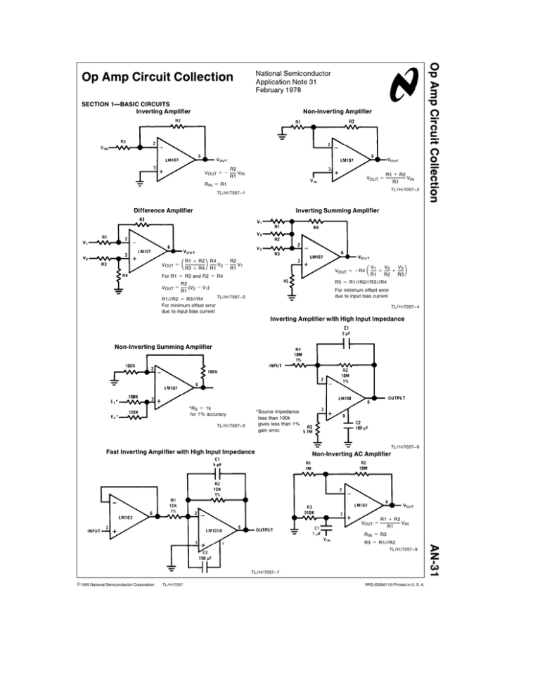
SECTION 1ÐBASIC CIRCUITS Inverting Amplifier Non-Inverting Amplifier VOUT e b R2 VIN R1 VOUT e RIN e R1 R1 a R2 VIN R1 TL/H/7057 – 2 TL/H/7057 – 1 Difference Amplifier VOUT e # R3 R1 a R2 a R4 Inverting Summing Amplifier J R1 V R4 2b R2 V1 R1 VOUT e b R4 For R1 e R3 and R2 e R4 VOUT e Op Amp Circuit Collection National Semiconductor Application Note 31 February 1978 Op Amp Circuit Collection # R1 V1 a V2 V a 3 R2 R3 R5 e R1UR2UR3UR4 R2 (V2 b V1) R1 J For minimum offset error due to input bias current TL/H/7057 – 3 R1UR2 e R3UR4 For minimum offset error due to input bias current TL/H/7057 – 4 Inverting Amplifier with High Input Impedance Non-Inverting Summing Amplifier *RS e 1k for 1% accuracy *Source Impedance less than 100k gives less than 1% gain error. TL/H/7057 – 5 TL/H/7057 – 6 Fast Inverting Amplifier with High Input Impedance Non-Inverting AC Amplifier VOUT e R1 a R2 VIN R1 RIN e R3 TL/H/7057 – 8 TL/H/7057 – 7 C1995 National Semiconductor Corporation TL/H/7057 RRD-B30M115/Printed in U. S. A. AN-31 R3 e R1UR2 Practical Differentiator Integrator fc e 1 2qR2C1 VOUT e b fh e 1 1 e 2qR1C1 2qR2C2 fc e 1 R1C1 1 2qR1C1 # t2 t1 VIN dt R1 e R2 fc m fh m funity gain For minimum offset error due to input bias current TL/H/7057–9 TL/H/7057 – 10 Fast Integrator Current to Voltage Converter VOUT e lIN R1 *For minimum error due to bias current R2 e R1 TL/H/7057 – 12 TL/H/7057 – 11 Circuit for Operating the LM101 without a Negative Supply Circuit for Generating the Second Positive Voltage TL/H/7057 – 14 TL/H/7057–13 2 Neutralizing Input Capacitance to Optimize Response Time Double-Ended Limit Detector CN s R1 CS R2 VOUT e 4.6V for VLT s VIN s VUT VOUT e 0V for TL/H/7057 – 15 VIN k VLT or VIN l VUT Integrator with Bias Current Compensation TL/H/7057 – 19 Multiple Aperture Window Discriminator *Adjust for zero integrator drift. Current drift typically 0.1, n/A§ C over b 55§ C to 125§ C temperature range. TL/H/7057 – 16 Voltage Comparator for Driving DTL or TTL Integrated Circuits TL/H/7057 – 17 Threshold Detector for Photodiodes TL/H/7057 – 20 TL/H/7057 – 18 3 Offset Voltage Adjustment for Inverting Amplifiers Using Any Type of Feedback Element Offset Voltage Adjustment for Non-Inverting Amplifiers Using Any Type of Feedback Element RANGE e g V RANGE e g V GAIN # J R2 R1 e1a # R1 J R2 R5 R4 a R2 TL/H/7057 – 22 TL/H/7057–21 Offset Voltage Adjustment for Voltage Followers RANGE e g V Offset Voltage Adjustment for Differential Amplifiers # R1 J R3 TL/H/7057–23 R2 e R3 a R4 RANGE e g V GAIN e R2 R1 Offset Voltage Adjustment for Inverting Amplifiers Using 10 kX Source Resistance or Less R1 e 2000 R3UR4 R4UR3 s 10 kX RANGE e g V 4 # R3UR4 R1 J TL/H/7057 – 25 # R4 J # R1 R5 R1 a R3 TL/H/7057 – 24 J SECTION 2 Ð SIGNAL GENERATION Low Frequency Sine Wave Generator with Quadrature Output TL/H/7057 – 26 High Frequency Sine Wave Generator with Quadrature Output fo e 10 kHz TL/H/7057 – 27 5 Free-Running Multivibrator Wein Bridge Sine Wave Oscillator R1 e R2 *Chosen for oscillation at 100 Hz C1 e C2 TL/H/7057–28 fe 1 2qR1 C1 *Eldema 1869 10V, 14 mA Bulb TL/H/7057 – 29 Function Generator TL/H/7057 – 30 Pulse Width Modulator TL/H/7057 – 31 6 Bilateral Current Source Bilateral Current Source IOUT e R3 VIN R1 R5 R3 e R4 a R5 R1 e R2 IOUT e R3 VIN R1 R5 R3 e R4 a R5 R1 e R2 TL/H/7057 – 32 TL/H/7057 – 33 Wein Bridge Oscillator with FET Amplitude Stabilization R1 e R2 C1 e C2 fe 1 2qR1 C1 TL/H/7057 – 34 7 Low Power Supply for Integrated Circuit Testing *VOUT e 1V/kX TL/H/7057 – 91 TL/H/7057–35 Positive Voltage Reference Positive Voltage Reference TL/H/7057 – 37 TL/H/7057–36 8 Negative Voltage Reference Negative Voltage Reference TL/H/7057 – 39 TL/H/7057 – 38 Precision Current Sink Precision Current Source VIN IO e R1 TL/H/7057 – 41 VIN t 0V TL/H/7057 – 40 SECTION 3 Ð SIGNAL PROCESSING Differential-Input Instrumentation Amplifier R4 R5 e R2 R3 AV e R4 R2 TL/H/7057 – 42 9 Variable Gain, Differential-Input Instrumentation Amplifier *Gain adjust AV e 10b4 R6 TL/H/7057 – 43 Instrumentation Amplifier with g 100 Volt Common Mode Range R3 e R4 R1 e R6 e 10R3 AV e R7 R6 * ² Matching determines common mode rejection. R1 e R5 e 10R2 R2 e R3 TL/H/7057 – 44 10 Instrumentation Amplifier with g 10 Volt Common Mode Range R1 e R4 R2 e R5 R6 e R7 ² *Matching Determines CMRR AV e # R6 2R1 1a R2 R3 J TL/H/7057 – 45 High Input Impedance Instrumentation Amplifier R1 e R4; R2 e R3 * ² Matching determines CMRR AV e 1 a ³ May be deleted to maximize bandwidth R1 R2 TL/H/7057 – 46 Bridge Amplifier with Low Noise Compensation *Reduces feed through of power supply noise by 20 dB and makes supply bypassing unnecessary. ²Trim for best common mode rejection ³Gain adjust TL/H/7057 – 47 11 Bridge Amplifier Precision Diode R1 R2 e RS1 RS2 VOUT e V a #1 b R1 RS1 J TL/H/7057–48 TL/H/7057 – 49 Precision Clamp Fast Half Wave Rectifier *EREF must have a source impedance of less than 200X if D2 is used. TL/H/7057–50 TL/H/7057 – 51 Precision AC to DC Converter *Feedforward compensation can be used to make a fast full wave rectifier without a filter. TL/H/7057 – 52 Low Drift Peak Detector TL/H/7057 – 53 12 Absolute Value Amplifier with Polarity Detector VOUT e b l VIN l c R2 R1 R2 R4 a R3 e R1 R3 TL/H/7057 – 54 Sample and Hold *Polycarbonate-dielectric capacitor TL/H/7057 – 55 Sample and Hold *Worst case drift less than 2.5 mV/sec ² Teflon, Polyethylene or Polycarbonate Dielectric Capacitor TL/H/7057 – 56 13 Low Drift Integrator TL/H/7057 – 57 *Q1 and Q3 should not have internal gate-protection diodes. Worst case drift less than 500 mV/sec over b 55§ C to a 125§ C. Fast ² Summing Amplifier with Low Input Current TL/H/7057 – 58 ² Power Bandwidth: 250 kHz * In addition to increasing speed, the LM101A raises high and low frequency gain, increases output drive capability and eliminates thermal feedback. Small Signal Bandwidth: 3.5 MHz Slew Rate: 10V/ms ³ C5 e 14 6 c 10b8 Rf Fast Integrator with Low Input Current TL/H/7057 – 59 Adjustable Q Notch Filter fO e 1 2qR1C1 e 60 Hz R1 e R2 e R3 C1 e C2 e C23 TL/H/7057 – 60 15 Easily Tuned Notch Filter Tuned Circuit fO e 1 2q0R1R2C1C2 TL/H/7057 – 62 R4 e R5 R1 e R3 R4 e (/2 R1 fO e 1 2qR40C1C2 TL/H/7057 – 61 Two-Stage Tuned Circuit fO e 1 2q0R1R2C1C2 TL/H/7057 – 63 16 Negative Capacitance Multiplier Ce R2 C1 R3 VOS a R2 IOS IL e R3 RS e R3(R1 a RIN) RIN AVO TL/H/7057 – 65 Variable Capacitance Multiplier Ce #1 a J Rb C1 Ra TL/H/7057 – 66 Simulated Inductor Capacitance Multiplier Ce R1 C1 R3 VOS a IOS R1 IL e R3 RS e R3 L t R1 R2 C1 RS e R2 RP e R1 TL/H/7057 – 67 TL/H/7057 – 68 17 High Pass Active Filter TL/H/7057 – 71 *Values are for 100 Hz cutoff. Use metalized polycarbonate capacitors for good temperature stability. Low Pass Active Filter TL/H/7057 – 72 *Values are for 10 kHz cutoff. Use silvered mica capacitors for good temperature stability. Nonlinear Operational Amplifier with Temperature Compensated Breakpoints TL/H/7057 – 73 18 Current Monitor Saturating Servo Preamplifier with Rate Feedback VOUT e R1 R3 IL R2 TL/H/7057 – 75 TL/H/7057–74 Power Booster TL/H/7057 – 76 19 Analog Multiplier R5 e R1 V1 t 0 # 10 J Vb V1 V2 VOUT e 10 TL/H/7057 – 77 Long Interval Timer Fast Zero Crossing Detector *Low leakage b 0.017 mF per second delay TL/H/7057 – 78 Amplifier for Piezoelectric Transducer TL/H/7057 – 79 Propagation delay approximately 200 ns ² DTL or TTL fanout of three. Minimize stray capacitance Pin 8 Temperature Probe *Set for 0V at 0§ C ² Adjust for 100 mV/§ C TL/H/7057 – 81 Low frequency cutoff e R1 C1 TL/H/7057–80 20 Photodiode Amplifier Photodiode Amplifier VOUT e R1 ID VOUT e 10 V/mA TL/H/7057 – 82 TL/H/7057 – 83 *Operating photodiode with less than 3 mV across it eliminates leakage currents. High Input Impedance AC Follower TL/H/7057 – 84 Temperature Compensated Logarithmic Converter ² 1 kX ( g 1%) at 25§ C, a 3500 ppm/§ C. Available from Vishay Ultronix, Grand Junction, CO, Q81 Series. *Determines current for zero crossing on output: 10 mA as shown. TL/H/7057 – 85 10 nA k IIN k 1 mA Sensitivity is 1V per decade 21 22 * ² 2N3728 matched pairs Root Extractor TL/H/7057 – 86 Multiplier/Divider TL/H/7057 – 87 Cube Generator TL/H/7057 – 88 23 Op Amp Circuit Collection Fast Log Generator ² 1 kX ( g 1%) at 25§ C, a 3500 ppm/§ C. Available from Vishay Ultronix, Grand Junction, CO, Q81 Series. TL/H/7057 – 89 Anti-Log Generator ² 1 kX ( g 1%) at 25§ C, a 3500 ppm/§ C. Available from Vishay Ultronix, Grand Junction, CO, Q81 Series. TL/H/7057 – 90 LIFE SUPPORT POLICY NATIONAL’S PRODUCTS ARE NOT AUTHORIZED FOR USE AS CRITICAL COMPONENTS IN LIFE SUPPORT DEVICES OR SYSTEMS WITHOUT THE EXPRESS WRITTEN APPROVAL OF THE PRESIDENT OF NATIONAL SEMICONDUCTOR CORPORATION. As used herein: AN-31 1. Life support devices or systems are devices or systems which, (a) are intended for surgical implant into the body, or (b) support or sustain life, and whose failure to perform, when properly used in accordance with instructions for use provided in the labeling, can be reasonably expected to result in a significant injury to the user. National Semiconductor Corporation 1111 West Bardin Road Arlington, TX 76017 Tel: 1(800) 272-9959 Fax: 1(800) 737-7018 2. A critical component is any component of a life support device or system whose failure to perform can be reasonably expected to cause the failure of the life support device or system, or to affect its safety or effectiveness. National Semiconductor Europe Fax: (a49) 0-180-530 85 86 Email: cnjwge @ tevm2.nsc.com Deutsch Tel: (a49) 0-180-530 85 85 English Tel: (a49) 0-180-532 78 32 Fran3ais Tel: (a49) 0-180-532 93 58 Italiano Tel: (a49) 0-180-534 16 80 National Semiconductor Hong Kong Ltd. 13th Floor, Straight Block, Ocean Centre, 5 Canton Rd. Tsimshatsui, Kowloon Hong Kong Tel: (852) 2737-1600 Fax: (852) 2736-9960 National Semiconductor Japan Ltd. Tel: 81-043-299-2309 Fax: 81-043-299-2408 National does not assume any responsibility for use of any circuitry described, no circuit patent licenses are implied and National reserves the right at any time without notice to change said circuitry and specifications.


