CMPA601C025F
25 W, 6.0 - 12.0 GHz, GaN MMIC, Power Amplifier
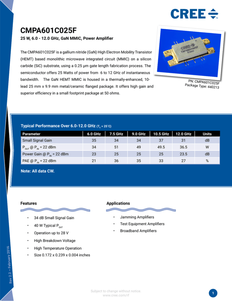
The CMPA601C025F is a gallium nitride (GaN) High Electron Mobility Transistor
(HEMT) based monolithic microwave integrated circuit (MMIC) on a silicon
carbide (SiC) substrate, using a 0.25 μm gate length fabrication process. The
semiconductor offers 25 Watts of power from 6 to 12 GHz of instantaneous
bandwidth.
The GaN HEMT MMIC is housed in a thermally-enhanced, 10-
PN: CMPA601C
025F
Package Type
: 440213
lead 25 mm x 9.9 mm metal/ceramic flanged package. It offers high gain and
superior efficiency in a small footprint package at 50 ohms.
Typical Performance Over 6.0-12.0 GHz (TC = 25˚C)
Parameter
6.0 GHz
7.5 GHz
9.0 GHz
10.5 GHz
12.0 GHz
Units
Small Signal Gain
35
34
34
37
31
dB
POUT @ PIN = 22 dBm
34
51
49
49.5
36.5
W
Power Gain @ PIN = 22 dBm
23
25
25
25
23.5
dB
PAE @ PIN = 22 dBm
21
36
35
33
27
%
Note: All data CW.
ry 2016
Rev 2.2 – Februa
Features
Applications
•
34 dB Small Signal Gain
•
Jamming Amplifiers
•
40 W Typical PSAT
•
Test Equipment Amplifiers
•
Operation up to 28 V
•
Broadband Amplifiers
•
High Breakdown Voltage
•
High Temperature Operation
•
Size 0.172 x 0.239 x 0.004 inches
Subject to change without notice.
www.cree.com/rf
1
Absolute Maximum Ratings (not simultaneous) at 25˚C
Parameter
Symbol
Rating
Units
Conditions
Drain-source Voltage
VDS
84
VDC
25˚C
Gate-source Voltage
VGS
-10, +2
VDC
25˚C
Storage Temperature
˚C
TSTG
-40, +150
Operating Junction Temperature
TJ
225
˚C
Maximum Forward Gate Current
IGMAX
23
mA
Soldering Temperature
TSTG
245
˚C
T
40
in-oz
RθJC
0.85
˚C/W
TC
-40, +150
˚C
1
Screw Torque
Thermal Resistance, Junction to Case2
Case Operating Temperature
2
25˚C
85˚C @ PDISS = 116 W
Note1 Refer to the Application Note on soldering at http://www.cree.com/rf/document-library
Note2 See also, the Power Dissipation De-rating Curve on page 4
Electrical Characteristics (Frequency = 6.0 GHz to 12.0 GHz unless otherwise stated; TC = 25˚C)
Characteristics
Symbol
Min.
Typ.
Max.
Units
Conditions
Gate Threshold
VTH
-3.8
-2.8
-2.3
V
VDS = 10 V, ID = 23 mA
Saturated Drain Current
IDS
10.6
13.0
–
A
VDS = 6V, VGS = 2 V
Drain-Source Breakdown Voltage
VBD
84
100
–
V
VGS = -8 V, IDS = 23 mA
Small Signal Gain
S21
28
31
–
dB
VDD = 28 V, IDQ = 2 A, PIN = -30 dBm
Output Power3,4
POUT1
45.5
47.2
–
dBm
VDD = 28 V, IDQ = 2 A, PIN = 22 dBm, Freq = 6 GHz
Output Power3,4
POUT2
45.5
47.1
–
dBm
VDD = 28 V, IDQ = 2 A, PIN = 22 dBm, Freq = 9.5 GHz
Output Power3,4
POUT3
43.7
45.5
–
dBm
VDD = 28 V, IDQ = 2 A, PIN = 22 dBm, Freq = 12 GHz
Power Added Efficiency3,4
PAE1
23
33.2
–
%
VDD = 28 V, IDQ = 2 A, PIN = 22 dBm, Freq = 6 GHz
Power Added Efficiency3,4
PAE2
26
32.3
–
%
VDD = 28 V, IDQ = 2 A, PIN = 22 dBm, Freq = 9.5 GHz
Power Added Efficiency3,4
PAE3
15.5
26.5
–
%
VDD = 28 V, IDQ = 2 A, PIN = 22 dBm, Freq = 12 GHz
Input Return Loss
S11
–
-5
–
dB
VDD = 28 V, IDQ = 2 A, PIN = -30 dBm
Output Return Loss
S22
–
-5
–
dB
VDD = 28 V, IDQ = 2 A, PIN = -30 dBm
VSWR
–
5:1
VSWR
Y
No damage at all phase angles,
VDD = 28 V, IDQ = 2 A, PIN = 22 dBm
DC Characteristics1,2
RF Characteristics3
Output Mismatch Stress
Notes:
1
Measured on-wafer prior to packaging.
2
Scaled from PCM data.
3
Measured in CMPA601C025F-AMP with 12.4 GHz low pass filter.
4
Fixture loss de-embedded using the following offsets. The offset is subtracted from the input offset value and added to the output offset value.
a) 6.0 GHz - 0.13 dB
b) 9.50 GHz - 0.26 dB
c) 12.0 GHz - 0.35 dB
Copyright © 2014-2016 Cree, Inc. All rights reserved. The information in this document is subject to change without notice. Cree and the Cree logo are
registered trademarks of Cree, Inc. Other trademarks, product and company names are the property of their respective owners and do not imply specific
product and/or vendor endorsement, sponsorship or association.
2
CMPA601C025F Rev 2.2
Cree, Inc.
4600 Silicon Drive
Durham, North Carolina, USA 27703
USA Tel: +1.919.313.5300
Fax: +1.919.869.2733
Fax: +1.919.869.2733
www.cree.com/RF
CMPA601C025F Typical Performance
Figure 1. - Small Signal S-Parameters vs. Frequency
VDD = 28 V, IDQ S-PARAMETER
= 2.0 A, PIN = -30 dBm
VDD=28V, IDQ=2.0A
50
40
30
Gain (dB)
20
10
0
-10
S11
-20
S21
S22
-30
5
6
7
8
9
10
11
Frequency (GHz)
12
13
14
15
Figure 2. - Output Power, Gain
and Power,
PowerPAE
Added
Output
and Efficiency
Power Gain vs. Input Power
Pin
=22
dBm,
VDD=28V,
VDD = 28 V, IDQ = 2.0 A, PIN = 22 IDQ=2.0A
dBm
60
55
Output Power (dBm), PAE(%) & Power Gain (dB)
50
45
40
35
30
25
20
15
POUT
10
PAE
PG
5
0
6
7
8
9
Frequency (GHz)
10
11
Copyright © 2014-2016 Cree, Inc. All rights reserved. The information in this document is subject to change without notice. Cree and the Cree logo are
registered trademarks of Cree, Inc. Other trademarks, product and company names are the property of their respective owners and do not imply specific
product and/or vendor endorsement, sponsorship or association.
3
CMPA601C025F Rev 2.2
12
Cree, Inc.
4600 Silicon Drive
Durham, North Carolina, USA 27703
USA Tel: +1.919.313.5300
Fax: +1.919.869.2733
Fax: +1.919.869.2733
www.cree.com/RF
CMPA601C025F Typical Performance
Figure 3. - Power Added Efficiency vs. Input Power
VDD =Added
28 V, Efficiency
IDQ = 2.0 Avs. Input power
Power
40
35
PAE (%)
30
25
20
15
6.0 GHz
9.5 GHz
12.0 GHz
10
8
10
12
14
16
18
Input Power (dBm)
20
22
24
26
Figure 4. - Output Power vs. Input Power
VDD = 28 V, IDQ = 2.0 A
Output power vs. Input power
50
48
Output Power (dBm)
46
44
42
40
6.0 GHz
9.5 GHz
12.0 GHz
38
36
8
10
12
14
16
18
Input Power (dBm)
20
22
Copyright © 2014-2016 Cree, Inc. All rights reserved. The information in this document is subject to change without notice. Cree and the Cree logo are
registered trademarks of Cree, Inc. Other trademarks, product and company names are the property of their respective owners and do not imply specific
product and/or vendor endorsement, sponsorship or association.
4
CMPA601C025F Rev 2.2
24
26
Cree, Inc.
4600 Silicon Drive
Durham, North Carolina, USA 27703
USA Tel: +1.919.313.5300
Fax: +1.919.869.2733
Fax: +1.919.869.2733
www.cree.com/RF
CMPA601C025F Typical Performance
Figure 5. - Gain vs Input Power
VDD = 28
V, vs.
IDQ Input
= 2.0 power
A
Gain
35
30
Power Gain (dB)
25
20
15
10
6.0 GHz
9.5 GHz
5
0
12.0 GHz
8
10
12
14
16
18
Input Power (dBm)
20
22
24
26
Figure
6. - PowerPower
Dissipation
Derating
Curve
CMPA601C025F
Dissipation
De-Rating
Curve
180
160
Power Dissipation (W)
140
Note 1
120
100
80
60
40
20
P…
0
0
25
50
75
100
125
150
175
200
225
250
Maximum Temperature (°C)
Note 1. Area exceeds Maximum Case Operating Temperature (See Page 2).
Copyright © 2014-2016 Cree, Inc. All rights reserved. The information in this document is subject to change without notice. Cree and the Cree logo are
registered trademarks of Cree, Inc. Other trademarks, product and company names are the property of their respective owners and do not imply specific
product and/or vendor endorsement, sponsorship or association.
5
CMPA601C025F Rev 2.2
Cree, Inc.
4600 Silicon Drive
Durham, North Carolina, USA 27703
USA Tel: +1.919.313.5300
Fax: +1.919.869.2733
Fax: +1.919.869.2733
www.cree.com/RF
CMPA601C025F-AMP Demonstration Amplifier Circuit Bill of Materials
Designator
Description
Qty
C2,C4,C5,C7,C9,C12
CAP,33000PF, 0805,100V, X7R
6
C1,C3,C6,C8,C10,C13
CAP, 1.0UF, 100V, 10%, X7R, 1210
6
C11,C14
CAP ELECT 3.3UF 80V FK SMD
2
R1,R2
RES 0.0 OHM 1/16W 0402 SMD
2
J1,J2
CONN, SMA, PANEL MOUNT JACK, FLANGE, 4-HOLE,
BLUNT POST, 20MIL
2
J3
HEADER RT>PLZ .1CEN LK 9POS
1
W1
WIRE, BLACK, 22 AWG ~ 1.50”
1
W2
WIRE, BLACK, 22 AWG ~ 1.75”
1
Q1
CMPA601C025F
1
CMPA601C025F-AMP Demonstration Amplifier Circuit
Copyright © 2014-2016 Cree, Inc. All rights reserved. The information in this document is subject to change without notice. Cree and the Cree logo are
registered trademarks of Cree, Inc. Other trademarks, product and company names are the property of their respective owners and do not imply specific
product and/or vendor endorsement, sponsorship or association.
6
CMPA601C025F Rev 2.2
Cree, Inc.
4600 Silicon Drive
Durham, North Carolina, USA 27703
USA Tel: +1.919.313.5300
Fax: +1.919.869.2733
Fax: +1.919.869.2733
www.cree.com/RF
CMP601C025F-AMP Demonstration Amplifier Circuit Schematic
CMPA601C025F-AMP Demonstration Amplifier Circuit Outline
Copyright © 2014-2016 Cree, Inc. All rights reserved. The information in this document is subject to change without notice. Cree and the Cree logo are
registered trademarks of Cree, Inc. Other trademarks, product and company names are the property of their respective owners and do not imply specific
product and/or vendor endorsement, sponsorship or association.
7
CMPA601C025F Rev 2.2
Cree, Inc.
4600 Silicon Drive
Durham, North Carolina, USA 27703
USA Tel: +1.919.313.5300
Fax: +1.919.869.2733
Fax: +1.919.869.2733
www.cree.com/RF
Product Dimensions CMPA601C025F
Pin Number
Qty
1
Gate Bias for Stage 1, 2 & 3
2
Gate Bias for Stage 1, 2 & 3
3
RF IN
4
Gate Bias for Stage 1, 2 & 3
5
Gate Bias for Stage 1, 2 & 3
6
Drain Bias
7
Drain Bias
8
RF OUT
9
Drain Bias
10
Drain Bias
Copyright © 2014-2016 Cree, Inc. All rights reserved. The information in this document is subject to change without notice. Cree and the Cree logo are
registered trademarks of Cree, Inc. Other trademarks, product and company names are the property of their respective owners and do not imply specific
product and/or vendor endorsement, sponsorship or association.
8
CMPA601C025F Rev 2.2
Cree, Inc.
4600 Silicon Drive
Durham, North Carolina, USA 27703
USA Tel: +1.919.313.5300
Fax: +1.919.869.2733
Fax: +1.919.869.2733
www.cree.com/RF
Part Number System
CMPA601C025F
Package
Power Output (W)
Upper Frequency (GHz)
Lower Frequency (GHz)
Cree MMIC Power Amplifier Product Line
Parameter
Value
Units
Lower Frequency
6.0
GHz
Upper Frequency1
12.0
GHz
25
W
Flanged
-
Power Output
Package
Table 1.
Note : Alpha characters used in frequency code
1
indicate a value greater than 9.9 GHz. See Table
2 for value.
Character Code
Code Value
A
0
B
1
C
2
D
3
E
4
F
5
G
6
H
7
J
8
K
9
Examples:
1A = 10.0 GHz
2H = 27.0 GHz
Table 2.
Copyright © 2014-2016 Cree, Inc. All rights reserved. The information in this document is subject to change without notice. Cree and the Cree logo are
registered trademarks of Cree, Inc. Other trademarks, product and company names are the property of their respective owners and do not imply specific
product and/or vendor endorsement, sponsorship or association.
9
CMPA601C025F Rev 2.2
Cree, Inc.
4600 Silicon Drive
Durham, North Carolina, USA 27703
USA Tel: +1.919.313.5300
Fax: +1.919.869.2733
Fax: +1.919.869.2733
www.cree.com/RF
Product Ordering Information
Order Number
Description
Unit of Measure
CMPA601C025F
GaN HEMT
Each
Test board without GaN HEMT
Each
Test board with GaN HEMT installed
Each
CMPA601C025F-TB
CMPA601C025F-AMP
Copyright © 2014-2016 Cree, Inc. All rights reserved. The information in this document is subject to change without notice. Cree and the Cree logo are
registered trademarks of Cree, Inc. Other trademarks, product and company names are the property of their respective owners and do not imply specific
product and/or vendor endorsement, sponsorship or association.
10
CMPA601C025F Rev 2.2
Image
Cree, Inc.
4600 Silicon Drive
Durham, North Carolina, USA 27703
USA Tel: +1.919.313.5300
Fax: +1.919.869.2733
Fax: +1.919.869.2733
www.cree.com/RF
Disclaimer
Specifications are subject to change without notice. Cree, Inc. believes the information contained within this data sheet to be accurate
and reliable. However, no responsibility is assumed by Cree for its use or for any infringement of patents or other rights of third parties
which may result from its use. No license is granted by implication or otherwise under any patent or patent rights of Cree. Cree makes
no warranty, representation or guarantee regarding the suitability of its products for any particular purpose. “Typical” parameters are the
average values expected by Cree in large quantities and are provided for information purposes only. These values can and do vary in
different applications, and actual performance can vary over time. All operating parameters should be validated by customer’s technical
experts for each application. Cree products are not designed, intended, or authorized for use as components in applications intended for
surgical implant into the body or to support or sustain life, in applications in which the failure of the Cree product could result in personal
injury or death, or in applications for the planning, construction, maintenance or direct operation of a nuclear facility. CREE and the CREE
logo are registered trademarks of Cree, Inc.
For more information, please contact:
Cree, Inc.
4600 Silicon Drive
Durham, North Carolina, USA 27703
www.cree.com/RF
Sarah Miller
Marketing
Cree, RF Components
1.919.407.5302
Ryan Baker
Marketing & Sales
Cree, RF Components
1.919.407.7816
Tom Dekker
Sales Director
Cree, RF Components
1.919.407.5639
Copyright © 2014-2016 Cree, Inc. All rights reserved. The information in this document is subject to change without notice. Cree and the Cree logo are
registered trademarks of Cree, Inc. Other trademarks, product and company names are the property of their respective owners and do not imply specific
product and/or vendor endorsement, sponsorship or association.
11
CMPA601C025F Rev 2.2
Cree, Inc.
4600 Silicon Drive
Durham, North Carolina, USA 27703
USA Tel: +1.919.313.5300
Fax: +1.919.869.2733
Fax: +1.919.869.2733
www.cree.com/RF
Mouser Electronics
Authorized Distributor
Click to View Pricing, Inventory, Delivery & Lifecycle Information:
Cree, Inc.:
CMPA601C025F-TB CMPA601C025F


