MP2002
Low Input Voltage
500mA Linear Regulator
The Future of Analog IC Technology
DESCRIPTION
FEATURES
The MP2002 is a low-current, low-dropout
linear regulator operating over a single input
supply between 1.35V to 6.5V. The output
voltage of the MP2002 is adjustable via an
external resistor divider. The MP2002 can
supply up to 500mA of load current. The enable
pin (EN) allows the part to be put into a low
current shutdown mode (EN=0). The MP2002
features thermal overload and current limit
protection. It is available in an 8-pin QFN (2 x
3mm) package
•
•
•
•
•
•
Power Good Open Collector Output
Operates from 1.35V – 6.5V Input
Low 300mV Dropout at 500mA Output
Stable with Very Small Ceramic Capacitors
2% Feedback Reference
Adjustable Output Voltage Option from 0.5V
to 5V using an External Resistor Divider
Better Than 0.001%/mA Load Regulation
Low 100μA Ground Current
Internal Thermal Protection
Current Limit Protection
6µA Typical Quiescent Current at Shutdown
Available in a Tiny 2 x 3mm 8-pin QFN
Package
•
•
•
•
•
•
APPLICATIONS
•
•
•
Low Current Regulators
Battery Powered Systems
Cellular Phones
All MPS parts are lead-free and adhere to the RoHS directive. For MPS green
status, please visit MPS website under Quality Assurance. “MPS” and “The
Future of Analog IC Technology” are Registered Trademarks of Monolithic
Power Systems, Inc.
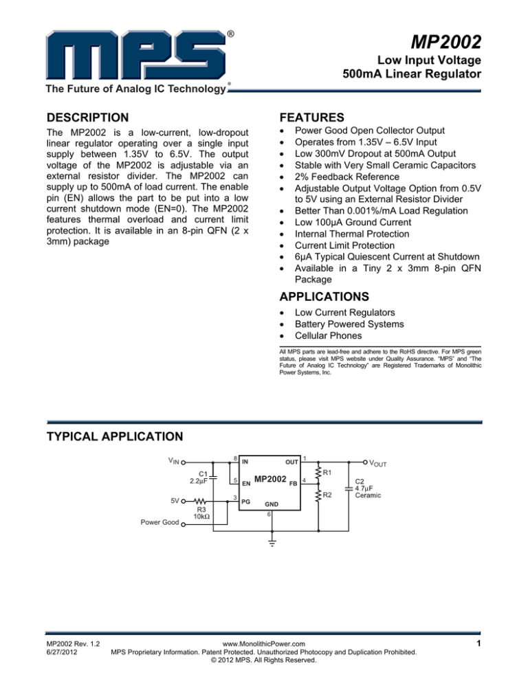
TYPICAL APPLICATION
VIN
8
5
5V
3
IN
EN
PG
OUT
MP2002
1
VOUT
R1
FB
4
R2
GND
6
Power Good
MP2002 Rev. 1.2
6/27/2012
www.MonolithicPower.com
MPS Proprietary Information. Patent Protected. Unauthorized Photocopy and Duplication Prohibited.
© 2012 MPS. All Rights Reserved.
1
MP2002 – LOW INPUT VOLTAGE, 500mA LINEAR REGULATOR
ORDERING INFORMATION
Part Number*
MP2002DD
Package
QFN8 (2 x 3mm)
Top Marking
L7
* For Tape & Reel, add suffix –Z (eg. MP2002DD–Z)
For RoHS Compliant Packaging, add suffix –LF (eg. MP2002DD–LF–Z)
PACKAGE REFERENCE
TOP VIEW
OUT
1
8
IN
NC
2
7
NC
PG
3
6
GND
FB
4
5
EN
EXPOSED PAD
ON BACKSIDE
Connect to GND
ABSOLUTE MAXIMUM RATINGS (1)
IN, PG, FB to GND..........................-0.3V to +7V
EN to GND .............................-0.3V to VIN +0.3V
OUT ......................................-0.3V to VIN + 0.3V
Continuous Power Dissipation
(TA = +25°C)(2)
……………………………………………….2.27W
Junction Temperature ...............................150°C
Lead Temperature ....................................260°C
Storage Temperature .............. -65°C to +150°C
Recommended Operating Conditions
(3)
Input Voltage VIN ...........................1.35V to 6.5V
Output Voltage ...................................0.5V to 5V
Load Current ...........................500mA Maximum
Operating Junction Temp. (TJ). -40°C to +125°C
MP2002 Rev. 1.2
6/27/2012
Thermal Resistance
(4)
θJA
θJC
QFN8 (2 x 3mm) .....................55 ...... 12 ... °C/W
Notes:
1) Exceeding these ratings may damage the device.
2) The maximum allowable power dissipation is a function of the
maximum junction temperature TJ(MAX), the junction-toambient thermal resistance θJA, and the ambient temperature
TA. The maximum allowable continuous power dissipation at
any ambient temperature is calculated by PD(MAX)=(TJ(MAX)TA)/ θJA. Exceeding the maximum allowable power dissipation
will cause excessive die temperature, and the regulator will go
into thermal shutdown. Internal thermal shutdown circuitry
protects the device from permanent damage.
3) The device is not guaranteed to function outside of its
operating conditions.
4) Measured on JESD51-7 4-layer board.
www.MonolithicPower.com
MPS Proprietary Information. Patent Protected. Unauthorized Photocopy and Duplication Prohibited.
© 2012 MPS. All Rights Reserved.
2
MP2002 – LOW INPUT VOLTAGE, 500mA LINEAR REGULATOR
ELECTRICAL CHARACTERISTICS
VIN = 1.8V, VOUT = 1.2V, COUT = 4.7µF, CIN = 2.2µF, TA = +25°C, unless otherwise noted.
Parameter
Operating Voltage
Ground Pin Current
Shutdown Current
Symbol Condition
IOUT = 1mA
IOUT = 1mA (7)
IOUT = 500mA
VEN = 0V, VIN = 5V
FB Regulation Voltage
–40°C ≤ TA ≤ +85°C
IOUT = 500mA
IOUT = 1mA,
VIN = (VOUT + 0.5V) to 6.5V (8)
IOUT = 1mA to 500mA,
VIN = VOUT + 0.5V
Dropout Voltage (8)
Line Regulation
Load Regulation
Power Good Output Voltage
Low(9)
EN Input High Voltage
EN Input Low Voltage
EN Input Bias Current
Thermal Protection
Current Limit
VOL
Min
1.35
0.482
0.477
Isink = 0.5mA
Typ (5)
100
5
7
0.500
0.495
290
Max
6.5
0.508
0.513
550
V
mV
0.005
%/V
0.001
%/mA
0.5
V
1.2
VEN = 1.5V, 5V
Units
V
µA
mA
µA
0.01
155
730
0.4
1
V
V
μA
°C
mA
Notes:
5) Parameter is guaranteed by design, not production tested.
6) Resistors for VOUT measurement are 10k, 14k, 1%
7) The ground current does not include current through feedback current
8) Dropout Voltage is defined as the input to output differential when the output voltage drops 1% below its nominal value
9) VFEEDBACK is 90% of the regulated value with 10k pull-up to 5V
MP2002 Rev. 1.2
6/27/2012
www.MonolithicPower.com
MPS Proprietary Information. Patent Protected. Unauthorized Photocopy and Duplication Prohibited.
© 2012 MPS. All Rights Reserved.
3
MP2002 – LOW INPUT VOLTAGE, 500mA LINEAR REGULATOR
TYPICAL PERFORMANCE CHARACTERISTICS
C1=2.2μF, C2 =4.7μF, C3=1nF, TA = +25°C, unless otherwise noted. (Reference Figure 2)
Voltage Dropout vs Current
0.40
VDROPOUT (V)
0.35
Line Regulation
Load Regulation
0.63
0.61
0.62
0.60
0.61
0.59
VIN=1.35V
VO=1.8V-3.3V
0.25
0.20
VO (V)
VO (V)
0.30
0.60
0.57
0.59
0.15
0.10
100
200
300
400
0.58
500
0.56
1
ILOAD CURRENT(mA)
85 ° C Load Regulation
0.58
2
3
4
5
INPUT VOLTAGE (V)
6
0
Line Regulation
1.83
1.804
1.81
1.82
1.80
1.81
VO (V)
VO (V)
1.796
1.79
VIN=5V
1.792
1.78
VIN=3.3V
1.788
200 300 400 500
ILOAD CURRENT (mA)
600
3.0
3.5
4.0
4.5
INPUT VOLTAGE (V)
0
5.0
Line Regulation
1.83
3.32
VO (V)
VIN=3.3V
VO (V)
3.3
VIN=5V
500
3.33
3.32
1.80
100
200
300 400
ILOAD CURRENT (mA)
Load Regulation
3.83
1.82
VIN=2.5V
1.78
2.5
-40 ° C Load Regulation
1.81
1.80
1.79
1.77
100
VO (V)
VO (V)
1.82
VIN=2.5V
500
Load Regulation
1.808
1.800
100
200
300 400
ILOAD CURRENT (mA)
3.30
3.31
VIN=3.6V
3.30
3.29
VIN=2.5V
1.79
1.78
0
100 200 300 400
500
ILOAD CURRENT (mA)
MP2002 Rev. 1.2
6/27/2012
3.29
3.28
600
0
3.5
3.28
3.9
4.3
4.7
5.1
INPUT VOLTAGE (V)
5.5
0
100
200
300 400
ILOAD CURRENT (mA)
www.MonolithicPower.com
MPS Proprietary Information. Patent Protected. Unauthorized Photocopy and Duplication Prohibited.
© 2012 MPS. All Rights Reserved.
500
4
MP2002 – LOW INPUT VOLTAGE, 500mA LINEAR REGULATOR
TYPICAL PERFORMANCE CHARACTERISTICS
C1=2.2μF, C2 =4.7μF, C3=1nF, TA = +25°C, unless otherwise noted. (Reference Figure 2)
Supply Current
Shut Down Current
Line Transient
VIN = 2V to 3V, VO = 1.8V, VEN= VIN,
ILOAD = 50mA, with Resisitor Load
170
10
160
9
150
8
140
7
130
6
120
VIN
0.5V/div.
VO
50mV/div.
5
1
2
3
4
5
6
1
INPUT VOLTAGE (V)
2
3
4
5
2 ms/div.
6
INPUT VOLTAGE (V)
PSRR vs Frequency
VFB vs Temperature
Load Transient
VIN = 2.5V, VO = 1.8V, VEN= VIN,
ILOAD = 50 to 300mA, with Resistor Load
VIN=1.8V, VEN=VIN, ILOAD=1mA
90
495.0
80
494.5
494.0
60
VFB (mV)
PSRR (dB)
70
50
40
30
20
VO
100mV/div.
493.5
ILOAD
0.2A/div.
493.0
492.5
10
0
492.0
0.1
1.0
10
100
1000
10000
FREQUENCY (Hz)
-50
-20
10
40
70
100
TEMPERATURE (C)
Enable Turn On
Power Good OFF
Enable Turn Off
VIN = 1.35V, VO = 0.6V, VEN = 0V to 3.6V,
VIN = 3.6V, VO = 1.8V,
VEN = VIN, ILOAD = 0.17A, with Resisitor Load ILOAD = 200mA, with Resistor Load
EN
2V/div.
PG
2V/div.
VO
1V/div.
VO
0.5V/div.
ILOAD
0.1A/div.
VIN = 1.35V, VO = 0.6V, VEN = 3.6V to 0V,
ILOAD = 200mA, with Resistor Load
EN
2V/div.
VO
0.5V/div.
ILOAD
0.2A/div.
ILOAD
0.2A/div.
1ms/div.
MP2002 Rev. 1.2
6/27/2012
www.MonolithicPower.com
MPS Proprietary Information. Patent Protected. Unauthorized Photocopy and Duplication Prohibited.
© 2012 MPS. All Rights Reserved.
5
MP2002 – LOW INPUT VOLTAGE, 500mA LINEAR REGULATOR
TYPICAL PERFORMANCE CHARACTERISTICS
C1=2.2μF, C2 =4.7μF, C3=1nF, TA = +25°C, unless otherwise noted. (Reference Figure 2)
Power Good ON
Thermal Protection
Short Circuit Protection
VIN = 2.5V, VO = 1.8V, VEN = VIN,
ILOAD = 0.3A, with Resistor Load
VIN = VEN = 5V,
VO = 1.8V, ILOAD = 0.5A
VIN = 4V, VO = 1.8V, VEN = VIN
VIN
2V/div.
PG
5V/div.
PG
2V/div.
VO
1V/div.
VO
1/div.
ILOAD
0.2A/div.
PG
2V/div.
VO
1V/div.
ILOAD
1A/div.
ILOAD
0.5/div.
1ms/div.
Short Circuit Recovery
VIN = 4V, VO = 1.8V, VIN = VEN
PG
2V/div.
VO
1V/div.
ILOAD
1A/div.
MP2002 Rev. 1.2
6/27/2012
www.MonolithicPower.com
MPS Proprietary Information. Patent Protected. Unauthorized Photocopy and Duplication Prohibited.
© 2012 MPS. All Rights Reserved.
6
MP2002 – LOW INPUT VOLTAGE, 500mA LINEAR REGULATOR
PIN FUNCTIONS
Pin #
Name
1
OUT
2
3
NC
PG
4
FB
5
EN
Description
Regulator Output. OUT is the output of the linear regulator. Bypass OUT to GND with
a 4.7μF or greater capacitor.
No connect.
Power Good Open Collector Output
Feedback Input. Connect a resistive voltage divider from OUT to FB to set the output
voltage. OUT feedback threshold is 0.5V.
Enable Input. Drive EN higher than 1.2V to turn on the MP2002, drive EN lower than
0.4V to turn it off.
7
GND,
Exposed
pad
NC
8
IN
6
Ground. Exposed pad must be connected to GND plane.
No connect.
Power Source Input. IN supplies the internal power to the MP2002 and is the source
of the pass transistor. Bypass IN to GND with a 2.2μF or greater capacitor.
OPERATION
PSRR such as wireless modems, pagers, and
cellular phones.
The MP2002 uses a PNP pass element and
features internal thermal shutdown and an
internal current limit circuit.
The MP2002 is a low-current, low-voltage, highPSRR, low-dropout, linear regulator. It is
intended for use in devices that require very low
voltage, low quiescent current power and high
OUT
VIN
8
VOUT
1
THERMAL
PROTECT
C1
R1
FB
--
4
R2
+
R3
5V
+
--
5
EN
PG
C2
0.5V
REF
6
3
GND
PG
Figure 1—Block Diagram of Ultra Low Noise Adjustable Output Regulator
MP2002 Rev. 1.2
6/27/2012
www.MonolithicPower.com
MPS Proprietary Information. Patent Protected. Unauthorized Photocopy and Duplication Prohibited.
© 2012 MPS. All Rights Reserved.
7
MP2002 – LOW INPUT VOLTAGE, 500mA LINEAR REGULATOR
APPLICATION INFORMATION
Setting the Output Voltage
The MP2002 has an adjustable output voltage,
set via an external resistor divider (R1 and R2
in Figure 2).
⎛V
− VFB
R1 = R2 × ⎜⎜ OUT
VFB
⎝
⎞
⎟⎟
⎠
where VFB = 0.5V (The OUT feedback threshold
voltage.)
Example: For 2.5V Output and R2=10kΩ
⎛ 2.5 − 0.5 ⎞
R1 = 10k × ⎜
⎟ = 40kΩ
⎝ 0.5 ⎠
A standard 40kΩ (±1%) resistor can be selected
for R1.
Table 1 lists the selected R1 values for some
typical output voltages (assuming R2 = 10kΩ).
Power Good
The power good pin is an open collector output
completed with a pull up resistor (10kΩ
recommended). The pull up resistor can be tied
to a supply within the voltage range of the pin
(0V to 5.5V). For example, the pull up resistor
can be tied to the input voltage when it is being
monitored by an IC powered from this input
voltage. It monitors the output voltage, and if
the output voltage is 10% below its regulation
point, the PG pin becomes low.
MP2002 Rev. 1.2
6/27/2012
Table 1—Adjustable Output Voltage R1 Values
(R2=10kΩ)
VOUT (V)
R1 (Ω)
1.25
15k
1.5
20k
1.8
26k
2
30k
2.5
40k
2.8
46k
3
50k
3.3
56k
4
70k
5
90k
Bypass Capacitors
For lower noise, the reference voltage can be
bypassed by an external capacitor. A low ESR
capacitor, such as the ceramic type, will provide
the best performance.
www.MonolithicPower.com
MPS Proprietary Information. Patent Protected. Unauthorized Photocopy and Duplication Prohibited.
© 2012 MPS. All Rights Reserved.
8
MP2002 – LOW INPUT VOLTAGE, 500mA LINEAR REGULATOR
PCB Layout Guide
PCB layout is very important to achieve good
regulation, ripple rejection, transient response
and thermal performance. It is highly
recommended to duplicate EVB layout for
optimum performance.
1)
If change is necessary, please follow these
guidelines and take Figure 2 for reference.
3)
8
VIN
C1
IN
5
3
EN
PG
R3
2)
OUT
MP2002
Input and output bypass ceramic capacitors
are suggested to be put close to the IN Pin
and OUT Pin respectively.
Ensure all feedback connections are short
and direct. Place the feedback resistors and
compensation components as close to the
chip as possible.
Connect IN, OUT and especially GND
respectively to a large copper area to cool
the chip to improve thermal performance and
long-term reliability.
1
1.8V
R1
FB
C3
4
R2
C2
GND
6
PG
C2
OUT
R1
R3
IN
C3
OUT
1
8
NC
2
7
NC
PG
3
6
GND
FB
4
5
EN
R2
IN
C1
GND
Top Layer
Bottom Layer
Figure 2—PCB Layout
MP2002 Rev. 1.2
6/27/2012
www.MonolithicPower.com
MPS Proprietary Information. Patent Protected. Unauthorized Photocopy and Duplication Prohibited.
© 2012 MPS. All Rights Reserved.
9
MP2002 – LOW INPUT VOLTAGE, 500mA LINEAR REGULATOR
TYPICAL APPLICATION CIRCUIT
8
VIN
5
3
IN
EN
PG
OUT
MP2002
1
C3
1nF
FB
1.8V
4
GND
6
PG
Figure 3—Typical Application Circuit with Fix Pinout
MP2002 Rev. 1.2
6/27/2012
www.MonolithicPower.com
MPS Proprietary Information. Patent Protected. Unauthorized Photocopy and Duplication Prohibited.
© 2012 MPS. All Rights Reserved.
10
MP2002 – LOW INPUT VOLTAGE, 500mA LINEAR REGULATOR
PACKAGE INFORMATION
QFN8 (2mm x 3mm)
2.90
3.10
PIN 1 ID
MARKING
0.30
0.50
0.18
0.30
1.90
2.10
PIN 1 ID
INDEX AREA
1.65
1.85
8
PIN 1 ID
SEE DETAIL A
1
1.50
1.70
0.50
BSC
4
5
TOP VIEW
BOTTOM VIEW
PIN 1 ID OPTION A
0.30x45” TYP.
0.80
1.00
PIN 1 ID OPTION B
R0.20 TYP.
0.20 REF
0.00
0.05
SIDE VIEW
DETAIL A
2.90
0.70
NOTE:
1.70
1) ALL DIMENSIONS ARE IN MILLIMETERS.
2) EXPOSED PADDLE SIZE DOES NOT INCLUDE MOLD FLASH.
3) LEAD COPLANARITY SHALL BE 0.10 MILLIMETER MAX.
4) DRAWING CONFORMS TO JEDEC MO-229, VARIATION VCED-2.
5) DRAWING IS NOT TO SCALE.
0.25
1.60
0.50
RECOMMENDED LAND PATTERN
NOTICE: The information in this document is subject to change without notice. Users should warrant and guarantee that third
party Intellectual Property rights are not infringed upon when integrating MPS products into any application. MPS will not
assume any legal responsibility for any said applications.
MP2002 Rev. 1.2
6/27/2012
www.MonolithicPower.com
MPS Proprietary Information. Patent Protected. Unauthorized Photocopy and Duplication Prohibited.
© 2012 MPS. All Rights Reserved.
11


