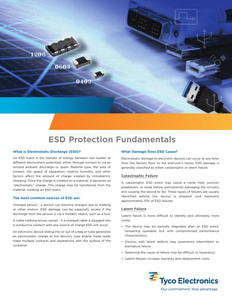
ESD Protection Fundamentals
What is Electrostatic Discharge (ESD)?
What Damage Does ESD Cause?
An ESD event is the transfer of energy between two bodies at
different electrostatic potentials, either through contact or via an
ionized ambient discharge or spark. Material type, the area of
contact, the speed of separation, relative humidity, and other
factors affect the amount of charge created by triboelectric
charging. Once the charge is created on a material, it becomes an
“electrostatic” charge. This charge may be transferred from the
material, creating an ESD event.
Electrostatic damage to electronic devices can occur at any time,
from the factory floor to the end-user’s home. ESD damage is
generally classified as either catastrophic or latent failure.
The most common sources of ESD are:
Charged person - a person can become charged due to walking
or other motion. ESD damage can be especially severe if the
discharge from the person is via a metallic object, such as a tool.
A cable rubbing across carpet - if a charged cable is plugged into
a conductive contact with any source of charge ESD will occur.
An electronic device sliding into or out of a bag or tube generates
an electrostatic charge as the device's case and/or metal leads
make multiple contacts and separations with the surface of the
container.
Catastrophic Failure
A catastrophic ESD event may cause a metal melt, junction
breakdown, or oxide failure, permanently damaging the circuitry
and causing the device to fail. These types of failures are usually
identified before the device is shipped, and represent
approximately 10% of ESD failures.
Latent Failure
Latent failure is more difficult to identify and ultimately more
costly.
• The device may be partially degraded after an ESD event,
remaining operable, but with compromised performance
characteristics.
• Devices with latent defects may experience intermittent or
premature failure.
• Detecting the cause of failure may be difficult or hazardous.
• Latent failures increase warranty and replacement costs.
ESD Suppression Technology
ESD suppression devices attempt to divert a potentially
damaging charge away from sensitive circuitry and help protect
the system from catastrophic failure. A variety of technologies
are used for ESD protection. As figure 1 illustrates, Tyco
Electronics' low-capacitance PESD devices are suitable for many
high-frequency applications.
Figure 1
PESD Principle of Operation
PESD devices provide lower capacitance than traditional MLV
(multilayer varistor) or TVS (transient voltage suppression) diode
technology, and their low-trigger voltage and low-clamping
voltage also helps protect sensitive electronic components as
shown in figure 2.
are very low, due to the physical gaps between the conductive
particles.
• Conductive particles are dispersed in a non-conductive matrix.
• The gaps between each particle behave like spark gaps when
a high voltage ESD pulse occurs.
• When the voltage of the pulse reaches the "trigger voltage"
these gaps spark over, creating a very low resistance path.
• In normal operation, the leakage current and the capacitance
Figure 2
ESD Suppression for High Data Rate Applications
• USB 2.0 & USB 3.0
• HDMI 1.3
Overvoltage Protection Considerations for USB 3.0 Applications
The USB 3.0 protocol was developed to provide higher transfer
Protection recommendations for USB 2.0 and USB 3.0 are shown below
rates and increased maximum bus power and increased device
in figures 4 and 5.
current draw, new power management features, and new cables
and connectors that are backward-compatible with USB 2.0
devices. The most significant change is that an additional physical
bus has been added in parallel with the existing USB 2.0 bus.
The USB 2.0 protocol allows for data transfer rates of up to
480Mbps and supports plug-and-play hot swappable installation
and operation. In comparison, the USB 3.0 specification allows for
data transfer rates of up to 5Gbps, with fall-back support for the
Figure 4
Protection Recommendation for USB 2.0
Figure 5
Protection Recommendation for USB 3.0
lower speed USB 2.0.
USB 3.0 adds five new pins to the connector
to support the new SuperSpeed interface:
USB3_TX (differential pair), GND, and
USB3_RX (differential pair), as shown in
Figure 3
figure 3.
The SuperSpeed interface of USB 3.0 requires lower capacitance
ESD protection than that of USB 2.0. Adding very low
capacitance devices is critical to minimize insertion loss. With a
For more information on circuit protection considerations for
typical capacitance of 0.20pF and flat insertion loss to >6GHz,
USB applications download these White Papers today:
PESD devices are capable of handling numerous ESD transients.
Coordinated Circuit Protection Strategies Help Prevent Damage
PESD devices are applicable for ESD protection on USB 2.0’s high-
to USB Charger Systems and Portable Electronics
speed D+ and D- signal lines and USB 3.0 SuperSpeed signal lines.
Circuit Protection Strategies for USB 3.0 (link when published)
-2-
Timing/Performance Considerations for Adding ESD Protection to HDMI Systems
The HDMI 1.3 standard brings improved color depth and audio
As shown in figure 7, silicon solutions have much higher
output, among other benefits, while doubling the previous HDMI
capacitance. Although their eye diagrams are commonly shown
data rate to 3.4Gbps per differential signal pair. Because of the
at 2.25GHz, or 1.48GHz to show compliance with 1080p 36- and
increased risk of cable discharge events and damaging pulses
24-bit color depths, their eye diagrams appear to encroach on
from the operating environment and connected peripherals,
the HDMI 1.3 specification, even at these speeds. This can lead to
aggressive ESD (electrostatic discharge) protection is essential.
increased board design constraints. Figure 8 shows a typical
HDMI circuit protection scheme utilizing PESD devices.
When adding ESD protection to HDMI systems it is important to
consider the impact of additional capacitance and inductance on
timing of the chosen device on the high-speed TMDS pairs. When
operating at up to 3.4GHz on the TMDS pair, any additional
impedance on the line can distort the signal, leading to:
• Greater difficulty in meeting the required eye diagrams for
rise times and signal levels,
• Additional constraints on board design, and
• Lower system level performance.
To minimize timing impact on these high speed lines, there are
four key technical considerations to be made regarding the ESD
Figure 6
protection device.
Eye diagram of Tyco Electronics’ 0.25pF PESD device
operating at 3.4GHz.
1. Low capacitance
2. Low insertion loss
3. Stable capacitance vs. frequency
4. A good layout that runs at 3.4GHz, with margin
HDMI’s timing performance is typically measured with eye
diagrams – a timing analysis tool used to provide an accurate
visual display of timing and level errors. The grey space in the
middle of the eye diagram represents the HDMI 1.3 specification.
As the lines encroach on the grey space, the less margin of error
there is. The eye width is a good measure of the amount of time
the data lines are stable, and if any errors are present. The eye
height measures the level, or amplitude, of the signal. Since
Figure 7
Silicon ESD protection device eye diagram at 1.48GHz.
HDMI’s TMDS pairs are differential signals, it is important to
minimize both differential and signal-to-ground capacitance to
ensure the rise and fall times of the signals are within
specification. Optimally, the capacitance should be as low as
possible to give designers as much margin as possible.
The eye diagram performance of Tyco Electronics’ 0.25pF PESD
device operating at 3.4GHz is shown in figure 6.
This diagram shows that when operating at 3.4GHz, the highest
speed prescribed by HDMI 1.3, there is a margin between rise and
fall times and signal level. When operating at lower speeds, the
eye diagram is ‘cleaner’ and provides additional margin, thus
Figure 8
easing design constraints.
Typical HDMI circuit protection scheme utilizing PESD devices
HDMI Reference Layout Helps Reduce Design and Test Time
Tyco Electronics’ HDMI 1.3 reference layout in figure 9 offers
Developed in conjunction with Efficere, Inc., a leader in high-
designers a solution that reduces the need to make tradeoffs
speed interface design, the reference layout exceeds the HDMI 1.3
between size, ESD protection performance, and the ease of
specifications for operation at 3.4Gbps for Impedance (TDR),
implementation.
-3-
Data Eye, and Far End Crosstalk. It has also been validated with
full-board performance (including connector, and mating to plug)
and has passed with margin at 3.4GHz.
The “cut and paste” layout is backward compatible with HDMI 1.0,
1.1 and 1.2 and includes optional overcurrent protection when
used in HDMI transmitters such as set top boxes, computers and
DVD players.
Tyco Electronics' PolySwitch nanoSMD features:
For more detailed information,
• HDMI 1.3 compliance test results include TDR and Eye Diagram.
click here to:
• Uses 4-layer board and 0603 & 0402 size PESD devices, and
nanoSMDC020F-2 PolySwitch overcurrent protection devices.
HDMI ESD Protection without
Sacrificing Performance
• PolySwitch nanoSMD devices can be easily removed for HDMI
receiver applications where overcurrent protection is not required.
Figure 9
HDMI 1.3 Reference Layout
Operational Characteristics
Capacitance vs. frequency in the PESD device is flat, and the
of the pulse. The bottom figure shows the current through the
device maintains a very low capacitance, as shown in figure 10.
PESD device – including shunt current – when the PESD is turned
on.
Figure 11 illustrates the performance characteristics of a PESD
device. In the top figure, the PESD will turn on when ESD voltage
reaches the PESD device’s trigger voltage. The ESD strike will be
clamped to the PESD device’s clamping voltage for the duration
Figure 11
Figure 10
Definitions
• Operating Voltage (VDC): Defined as DC voltage under which
device is in OFF state and leakage current is below a certain
threshold.
• Leakage Current (IL): Current through device under Operating
Voltage VDC
• Trigger Voltage (Vt): Voltage at which the device switches
from the OFF to the ON state, during the IEC waveform or the
TLP (Transition Line Pulse) test system.
• Clamping Voltage (Vc): Voltage across device under 8 kV per
IEC or measured by TLP test system. Typically measured 30 ns
after initiation of the IEC ESD pulse, but 30ns and 60ns are
sometimes used for TLP.
• Capacitance (Cp): Capacitance of the device measured at 1
MHz with 0 bias and 1 Vrms signal.
Figure 12
-4-
ESD Suppressor Design Criteria
When specifying an ESD suppressor, the following design and
placement considerations should be made:
1. Data signal ground (GND) and Vbus transients must be
suppressed for proper operation.
3. Having both grounds connected on the board level may allow
transients to propagate via the signal ground with respect to
chassis ground. This may be especially critical when cables are
inserted into a USB connector.
4. To optimize ESD suppression, suppressor devices should be
2. Good design practices mandate that data signal ground and
chassis ground not be tied together at the board level.
Decoupling capacitors between Vbus and chassis ground
should be used to minimize EMC issues.
installed as close to the source of the ESD transient as possible.
The Tyco Electronics Product Advantage
• PESD devices help shunt ESD away from sensitive circuitry and
provide low capacitance compared to traditional MLV (multi
layer varistor) or TVS (transient voltage suppression) diode
technology.
• The PESD device's low capacitance, low-voltage clamping
levels, and high ESD tolerance are critical performance
parameters for high data-rate transmission applications
• The device's form factor meets the board-space and surface
mount installation requirements of new portable electronics
designs.
• PESD devices perform better than other comparable
components in transmission line pulse (TLP) testing, as well as
IEC61000-4-2 testing, especially after multiple hits (up to
1000).
Designs for a Smaller World
The electronics industry’s unrelenting demand for smaller, more
reliable circuit protection devices continues to drive the
miniaturization trend. Tyco Electronics consistently leads the
industry with smaller and smaller devices, but the objective is
more than size reduction. The real challenge lies in scaling down
component size without sacrificing electrical characteristics.
Investment in material research and technology has enabled the
development of devices that meet existing performance levels
within new, smaller, and more convenient packages.
Raychem Circuit Protection Products
308 Constitution Drive, Building H
Menlo Park, CA USA 94025-1164
Tel : (800) 227-7040, (650) 361-6900
Fax : (650) 361-4600
PolySwitch, Raychem, TE (logo) and Tyco Electronics are trademarks of Tyco Electronics group of companies
and its licensors. All information, including illustrations, is believed to be reliable. Users, however, should
independently evaluate the suitability of each product for their application. Tyco Electronics Corporation
makes no warranties as to the accuracy or completeness of the information, and disclaims any liability
regarding its use. Tyco Electronics’ only obligations are those in the Tyco Electronics Standard Terms and
Conditions of Sale for this product, and in no case will Tyco Electronics be liable for any incidental, indirect,
or consequential damages arising from the sale, resale, use, or misuse of the product. Specifications are
subject to change without notice. In addition, Tyco Electronics reserves the right to make changes without
notification to Buyer—to materials or processing that do not affect compliance with any applicable
specification.
© 2009 Tyco Electronics Corporation. All rights reserved. RCP0058E.1209
www.circuitprotection.com
www.circuitprotection.com.hk (Chinese)
www.tycoelectronics.com/japan/raychem (Japanese)


