ALM-11236
1710 MHz – 1850 MHz
Low Noise, High Linearity Amplifier Module
with Fail-Safe Bypass Feature
Data Sheet
Description
Features
Avago Technologies’ ALM-11236 is an easy-to-use GaAs
MMIC Tower Mount Amplifier (TMA) LNA Module with low
IL bypass path. The module has low noise and high linearity
achieved through the use of Avago Technologies’ proprietary 0.25 mm GaAs Enhancement-mode pHEMT process.
All matching components are fully integrated within the
module and the 50 ohm RF input and output pins are
already internally AC-coupled. This makes the ALM-11236
extremely easy to use as the only external parts are DC
supply bypass capacitors. For optimum performance
at other bands, ALM-11036 (776-870 MHz), ALM-11136
(870-915 MHz) and ALM-11336 (1850-1980) are recommended. All ALM-11x36 share the same package and pin
out configuration.
• Very Low Noise Figure
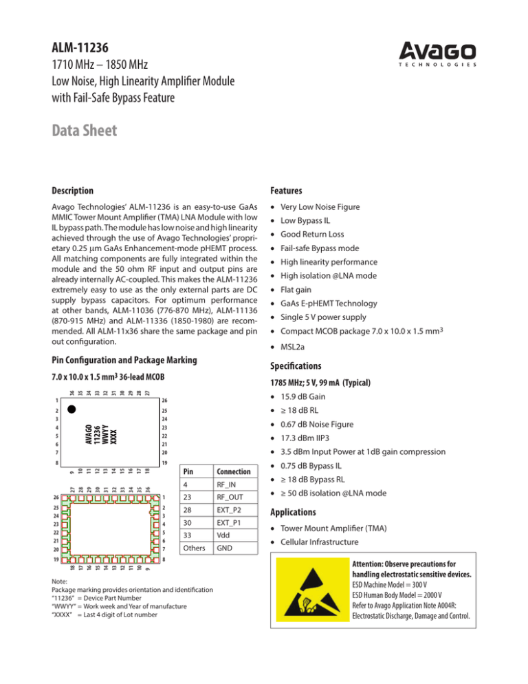
Pin Configuration and Package Marking
25
24
23
22
21
20
AVAGO
11236
WWYY
XXXX
2
3
4
5
6
7
8
27
28
29
30
31
32
33
34
35
36
9
10
11
12
13
14
15
16
17
18
19
• Fail-safe Bypass mode
• High linearity performance
• High isolation @LNA mode
• Flat gain
• GaAs E-pHEMT Technology
• Single 5 V power supply
• Compact MCOB package 7.0 x 10.0 x 1.5 mm3
• MSL2a
1785 MHz; 5 V, 99 mA (Typical)
36
35
34
33
32
31
30
29
28
27
26
• Good Return Loss
Specifications
7.0 x 10.0 x 1.5 mm3 36-lead MCOB
1
• Low Bypass IL
• 15.9 dB Gain
• ≥ 18 dB RL
• 0.67 dB Noise Figure
• 17.3 dBm IIP3
• 3.5 dBm Input Power at 1dB gain compression
Pin
Connection
4
RF_IN
• 0.75 dB Bypass IL
• ≥ 18 dB Bypass RL
1
23
RF_OUT
• ≥ 50 dB isolation @LNA mode
25
24
23
22
21
20
2
3
4
5
6
7
28
EXT_P2
30
EXT_P1
Applications
33
Vdd
Others
GND
19
8
18
17
16
15
14
13
12
11
10
9
26
Note:
Package marking provides orientation and identification
“11236” =Device Part Number
“WWYY”= Work week and Year of manufacture
“XXXX” =Last 4 digit of Lot number
• Tower Mount Amplifier (TMA)
• Cellular Infrastructure
Attention: Observe precautions for
handling electrostatic sensitive devices.
ESD Machine Model = 300 V
ESD Human Body Model = 2000 V
Refer to Avago Application Note A004R:
Electrostatic Discharge, Damage and Control.
Absolute Maximum Rating [1] TA = 25° C
Symbol
Parameter
Units
Absolute Max.
Vdd
Device Voltage,
RF output to ground
V
5.5
Pin,max
CW RF Input Power
(Vdd = 5.0 V, Idd = 100 mA)
dBm
+15
Pdiss
Total Power Dissipation [3]
W
0.715
Tj
Junction Temperature
°C
150
TSTG
Storage Temperature
°C
-65 to 150
Thermal Resistance [2]
(Vdd = 5.0 V, Idd = 100 mA) θjc = 56.2 °C/W
Notes:
1.Operation of this device in excess of any of
these limits may cause permanent damage.
2. Thermal resistance measured using Infra-Red
Measurement Technique.
3. Power dissipation with unit turned on. Board
temperature Tc is 25° C. Derate at 17.8 mW/°C
for Tc > 109.8 ° C.
Electrical Specifications [1, 4]
RF performance at TA = 25° C, Vdd = 5 V, 1785 MHz, measured on demo board in Figure 1 with component listed in Table1
for DC bypass.
Symbol
Parameter and Test Condition
Idd
Drain Current
Gain
Gain
IRL
Input Return Loss, 50 Ω source
ORL
Output Return Loss, 50 Ω load
NF [2]
Noise Figure
IIP3 [3]
IP1dB
Bypass IL
Bypass Insertion Loss, 50 Ω load Vdd = 0 V
Bypass IRL
Frequency (MHz)
Units
Min.
Typ.
Max.
mA
81
99
117
dB
–
14.5
16
15.9
–
17.5
dB
–
30
–
dB
–
28
–
dB
–
–
0.75
0.67
–
0.85
Input Third Order Intercept Point
dBm
14
17.3
–
Input Power at 1 dB Gain Compression
dBm
2.55
3.5
–
dB
–
0.75
1.1
Input Return Loss, 50 Ω source Vdd = 0 V
dB
–
19
–
Bypass ORL
Output Return Loss, 50 Ω load Vdd = 0 V
dB
–
23
–
ISOL
Bypass Isolation @LNA ON Vdd = 5 V
dB
–
56
–
1710
1785
1710
1785
1785
Notes:
1. Measurements at 1785 MHz obtained using demo board described in Figure 1.
2. For NF data, board losses of the input have not been de-embedded.
3. IIP3 test condition: FRF1 = 1785 MHz, FRF2 = 1786 MHz with input power of -15 dBm per tone.
4. Use proper bias, heatsink and derating to ensure maximum channel temperature is not exceeded. See absolute maximum ratings and application
note for more details.
2
Product Consistency Distribution Charts[1, 2]
LSL
80
USL
85
90
95
100
105
110
115
Figure 1. Idd, LSL = 81 mA , nominal = 99 mA, USL = 117 mA
15
0.7
0.8
Figure 3. NF, nominal = 0.67 dB, USL = 0.85 dB
16
17
Figure 2. Gain, LSL = 14.5 dB, nominal = 15.9 dB, USL = 17.5 dB
LSL
USL
0.6
USL
LSL
13
14
15
16
17
18
19
20
21
22
23
Figure 4. IIP3, LSL = 14 dBm, nominal = 17.3 dBm
LSL
LSL
3
Figure 5. IP1dB, LSL = 2.55 dBm, nominal = 3.5 dBm
4
-1.1
-1
-0.9
-0.8
-0.7
-0.6
Figure 6. Bypass IL, LSL = 1.1 dB, nominal = 0.75 dB
Notes:
1. Distribution data sample size is 1500 samples taken from 3 different wafer lots. Future wafers allocated to this product may have nominal values
anywhere between the upper and lower limits.
2. Circuit trace losses have not been de-embedded from measurements above.
3
Vsupply
GND
Demo Board Layout
Avago
Technologies
Z1
C1
Z2
27 Gnd
28 EXT_P2
30 EXT_P1
31 Gnd
32 Gnd
34 Gnd
33 Vdd
35 Gnd
36 Gnd
C3
29 Gnd
C2
ALM-
17
18
Gnd
Gnd
19 Gnd
16
8
Gnd
20 Gnd
Gnd
15
7
Gnd
21 Gnd
Gnd
14
6
13
22 Gnd
Gnd
Gnd
5
Gnd
23 RF_OUT
Gnd
12
4
Gnd
24 Gnd
RF_IN
11
25 Gnd
3
10
2
Gnd
Gnd
Gnd
Gnd
26 Gnd
9
1
Gnd
Gnd
rev1gi
March'10
Low T.M.
MILS
W 21.89
G 14.57
H 10
S 60
Figure 7. Demo Board Layout Diagram
– Recommended PCB material is 10 mils Rogers RO4350.
– Suggested component values may vary according to layout and PCB material.
– Copper trace between the 2 pads is removed before Z2 0(ohm) is placed.
4
Demo Board Schematic
Vdd (5 V)
Z1
Z2
C1
C2
27,29,31,32,34,35,36
EXT_P1
33
EXT_P2
28
30
1,2,3
24,25,26
BIAS
5V
4
50 Ω TL
RFin
5V
RFout
0V
19,20,21,22
5,6,7,8
9,10,11,12,13,14,15,16,17,18
Module Outline,
7 mm x 10 mm
Truth Table
Vdd (V)
LNA Mode
5
Bypass Mode
0
Fail-safe Mode
NC
Bypass and Fail-safe mode have similar performance
Figure 8. Demo Board Schematic Diagram
Table 1. DC component list for 1710-1850 MHz
Part
Size
Value
Detail Part Number
C1
0805
2.2 mF (Murata)
GRM21BR61E225KA12L
C2
0402
NU
NU
Z1
0805
0 Ω (Kamaya)
RMC1/8-JPTP
Z2
0603
0 Ω (Kamaya)
RMC1/16-JPTP
Notes:
C1 is a DC bypass capacitor.
Z1 is 0 Ω resistor or fuse.
Z2 is a 0 Ω resistor if an external function block is not used.
5
23
Typical Performance
RF performance at TA = 25° C, Vdd = 5 V for LNA mode, Vdd = 0 V for Bypass mode, measured on demo board in Figure 7.
Signal = CW unless stated otherwise. Application Test Circuit is shown in Figure 8 and Table 1. IIP3 test condition: FRF1-FRF2
= 1 MHz with input power of -15 dBm per tone.
110
17.0
16.5
16.0
Gain (dB)
Idd (mA)
105
100
95
15.5
15.0
14.5
14.0
85° C
25° C
-40° C
13.5
90
-40 -30 -20 -10 0
13.0
1.71
10 20 30 40 50 60 70 80 90
Temperature (°C)
Figure 9. Idd vs Temperature
1.83
1.85
-15
-20
-25
-15
-20
-25
-30
-30
-35
-35
1.73
1.75
1.77
1.79
Frequency (GHz)
1.81
1.83
-40
1.71
1.85
1.0
0.9
IIP3 (dBm)
0.8
0.7
0.6
0.5
85° C
25° C
-40° C
0.4
1.75
Figure 13. NF vs Frequency
1.73
1.75
1.77
1.79
Frequency (GHz)
1.81
1.83
1.85
Figure 12. S22 vs Frequency
1.1
1.73
85° C
25° C
-40° C
-10
Figure 11. S11 vs Frequency
NF(dB)
1.81
-5
S22 (dB)
S11 (dB)
-10
6
1.77 1.79
Frequency (GHz)
0
85° C
25° C
-40° C
-5
0.3
1.71
1.75
Figure 10. Gain vs Frequency
0
-40
1.71
1.73
1.77
1.79
Frequency (GHz)
1.81
1.83
1.85
30
28
26
24
22
20
18
16
14
12
10
1.71
85° C
25° C
-40° C
1.73
1.75
Figure 14. IIP3 vs Frequency
1.77
1.79
Frequency (GHz)
1.81
1.83
1.85
8.0
-0.5
85° C
25° C
-40° C
7.0
-0.7
5.0
Bypass IL (dB)
IP1dB(dBm)
6.0
4.0
3.0
1.0
-1.1
1.73
1.75
1.77
1.79
Frequency (GHz)
1.81
1.83
-1.2
1.71
1.85
1.77
1.79
Frequency (GHz)
1.81
1.83
1.85
85° C
25° C
-40° C
-5
Bypass S22 (dB)
Bypass S11 (dB)
-10
-15
-20
-25
-30
-10
-15
-20
-25
-30
1.73
1.75
1.77
1.79
Frequency (GHz)
1.81
1.83
1.85
Figure 17. Bypass S11 vs Frequency
85° C
25° C
-40° C
-35
-40
-45
-50
-55
-60
-65
1.73
1.75
1.77
1.79
Frequency (GHz)
Figure 19. Bypass isolation vs Frequency (LNA mode)
-35
1.71
1.73
1.75
1.77
1.79
Frequency (GHz)
Figure 18. Bypass S22 vs Frequency
-30
-70
1.71
1.75
0
85° C
25° C
-40° C
-5
-35
1.71
1.73
Figure 16. Bypass IL vs Frequency
0
Isolation (dB)
-0.9
-1.0
Figure 15. IP1dB vs Frequency
7
-0.8
2.0
0.0
1.71
85° C
25° C
-40° C
-0.6
1.81
1.83
1.85
1.81
1.83
1.85
Typical Scattering Parameters, Vdd = 5 V, Idd = 99 mA
LNA SPAR (100 MHz – 20 GHz)
Freq
(GHz)
S11
(dB)
S11
(ang)
S21
(dB)
S21
(ang)
S12
(dB)
S12
(ang)
S22
(dB)
S22
(ang)
0.1
-3.25
-107.27
-23.21
-79.05
-22.71
-83.91
-1.16
-65.01
0.5
-3.00
-169.55
-11.32
-88.29
-10.54
-79.80
-5.26
-170.06
1
-4.24
140.37
-12.52
147.68
-12.20
149.76
-7.02
119.52
1.5
-12.31
48.40
12.40
-37.49
-36.01
-46.99
-10.56
161.54
1.6
-16.97
65.15
15.44
-128.51
-34.00
-136.60
-25.65
11.73
1.7
-24.07
79.01
15.94
162.18
-31.68
157.19
-27.03
-148.51
1.72
-25.53
90.10
15.94
150.13
-31.32
146.21
-26.64
-148.30
1.74
-26.23
104.40
15.92
138.54
-31.04
135.63
-25.93
-144.76
1.76
-26.14
119.48
15.88
127.32
-30.78
125.75
-24.72
-141.40
1.78
-25.51
131.31
15.82
116.42
-30.57
115.93
-23.13
-140.89
1.80
-24.77
139.58
15.77
105.87
-30.40
106.49
-21.62
-142.37
1.82
-24.18
144.53
15.70
95.58
-30.24
97.60
-20.37
-145.83
1.84
-23.71
147.79
15.63
85.55
-30.11
88.69
-19.36
-151.26
1.86
-23.44
151.28
15.55
75.76
-29.98
79.99
-18.62
-157.63
1.88
-23.33
155.76
15.48
66.17
-29.90
71.62
-18.02
-164.51
1.90
-23.41
161.23
15.41
56.71
-29.81
63.13
-17.65
-171.55
1.92
-23.59
167.76
15.34
47.39
-29.71
54.92
-17.59
-178.29
1.94
-23.59
175.53
15.27
38.18
-29.64
46.64
-17.84
175.32
1.96
-23.18
-176.41
15.21
29.02
-29.56
38.56
-18.44
168.54
1.98
-22.22
-168.72
15.14
19.89
-29.48
30.36
-19.45
161.59
2
-20.96
-162.17
15.07
10.72
-29.40
21.97
-20.99
155.47
2.5
-15.00
162.88
6.07
162.87
-34.37
-156.98
-3.73
114.98
3
-10.85
-154.58
-9.49
22.90
-43.57
128.72
-1.97
-78.44
3.5
-6.81
-166.19
-23.86
-50.01
-47.26
107.79
-1.36
-158.06
4
-5.38
-179.92
-33.62
-105.76
-48.74
93.11
-1.52
149.58
4.5
-5.20
167.33
-42.09
154.80
-39.86
71.68
-1.80
99.28
5
-5.49
151.70
-37.16
0.38
-35.36
-9.63
-2.32
47.18
5.5
-6.50
138.34
-39.64
-74.83
-39.79
-15.82
-2.65
-24.58
6
-9.04
138.64
-36.13
-123.84
-28.33
-59.33
-2.46
-112.48
7
-0.87
133.48
-35.53
82.60
-30.74
56.93
-1.19
138.77
8
-0.72
98.99
-32.61
14.23
-33.29
10.82
-0.91
81.55
9
-1.08
75.89
-42.13
-63.92
-46.94
-78.34
-0.84
24.04
10
-2.94
40.90
-32.76
-28.80
-30.96
-21.81
-1.01
-12.07
11
-8.17
56.49
-31.07
-138.74
-29.87
-166.30
-1.97
-40.53
12
-5.11
5.66
-27.00
95.32
-27.61
92.07
-2.41
-68.06
13
-4.98
-12.88
-22.34
-34.76
-21.84
-29.64
-2.19
-96.12
14
-4.67
-42.69
-27.80
176.43
-27.00
-169.90
-2.02
-124.43
15
-20.78
-13.30
-26.22
-120.01
-27.34
-125.25
-3.33
-164.81
16
-11.64
25.55
-24.57
76.02
-23.99
75.45
-7.91
20.18
17
-6.43
-45.98
-18.99
4.64
-18.62
3.85
-4.86
-95.73
18
-6.65
-74.39
-28.60
-111.22
-27.51
-115.30
-11.29
-153.90
19
-2.22
-90.91
-28.40
-103.98
-28.35
-105.75
-3.64
-129.24
20
-4.95
-112.35
-15.78
168.58
-15.77
168.73
-10.94
-140.02
8
PCB Layout and Stencil Design
9.795
9.765
0.845 (pitch)
0.50
3.65
0.845
(pitch)
6.770
4.50
0.47
1.0375
6.80
5.20
0.50
8.10
0.20
1.0375
Pin 1
0.845
(pitch)
Pin 1
0.845 (pitch)
0.47
Stencil Opening
Land Pattern
0.845
0.845
(pitch)
Pin 1
1.0375
Metal
Combination of Land Pattern and Stencil Opening
Part Number Ordering Information
Part Number
No. of Devices
Container
ALM-11236-TR1G
1000
13” Reel
ALM-11236-BLKG
100
antistatic bag
9
Soldermask Open
Note :
1. Recommended Land Pattern & Stencil Opening.
2. Stencil thickness is 0.1 mm (4 mils)
3. All dimension are in MM unless otherwise specified
MCOB 7 x 10 Package Dimensions
Pin1 Identification
10.00±0.10
AVAGO
12236
WWYY
XXXX
1.50±0.10
7.00±0.10
1.12
Top View
0.50
Side View
0.845 (pitch)
Pin 1
0.50
0.10
0.05
(SM to metal gap)
0.845 (pitch)
R0.15
5.20
Bottom SM
8.10
Bottom Metal
1.0375
Notes:
1. All dimensions are in milimeters
2. Dimensions are inclusive of plating
3. Dimensions are exclusive of mold flash and metal burr
Bottom View
Device Orientation
REEL
USER FEED DIRECTION
CARRIER
TAPE
AVAGO
11236
WWYY
XXXX
TOP VIEW
USER
FEED
DIRECTION
COVER TAPE
10
AVAGO
11236
WWYY
XXXX
AVAGO
11236
WWYY
XXXX
END VIEW
Tape Dimensions
12.00 ± 0.10
2.00 ± 0.10
4.00 ± 0.10
1.75 ± 0.10
Ø 1.50 + 0.10
11.50 ± 0.10
24.00 + 0.30
− 0.10
Ø 1.50 + 0.25
0.318 ± 0.02
5° MAX
8° MAX
7.32 ± 0.10
A.
11
10.49 ± 0.10
2.06 ± 0.10
K.
B.
Reel Dimensions - 13” Reel
ESD Label
(See Below)
Recycle Symbol
Detail ‘X’
Embossed Line X2
90.0mm Length
Lines 147.0mm away from center point
Embossed ‘M’ 5.0mm Height
FRONT VIEW
Ø20.2 (Min)
25.65±1.75**
25.4±1.0*
Recycle Symbol
+0.5
Ø13.1 -0.2
2.2±0.5
See Detail ‘X’
FRONT
BACK
Ø100.0±0.5
Ø331.5 Max
Detail ‘X’
1.0
BACK VIEW
Detail ‘Y’
Slot 10.0±0.5(2x)
Slot 5.0±0.5***(1x)
4.0
30.4*
Max
For product information and a complete list of distributors, please go to our web site: www.avagotech.com
Avago, Avago Technologies, and the A logo are trademarks of Avago Technologies in the United States and other countries.
Data subject to change. Copyright © 2005-2013 Avago Technologies. All rights reserved.
AV02-2848EN - June 18, 2013
Detail ‘Y’
(Slot Hole)


