ADA-4643
Silicon Bipolar Darlington Amplifier
Data Sheet
Description
Features
Avago Technologies’ ADA-4643 is an economical, easy-touse, general purpose silicon bipolar RFIC gain block amplifiers housed in a 4-lead SC-70 (SOT-343) surface mount
plastic package which requires only half the board space
of a SOT-143 package.
Small Signal gain amplifier
Operating frequency DC – 2.5 GHz
Unconditionally stable
50 Ohms input & output
Flat, Broadband Frequency Response up to 1 GHz
Operating Current: 20 to 60 mA
Industry standard SOT-343 package
Lead-free option available
The Darlington feedback structure provides inherent
broad bandwidth performance, resulting in useful operating frequency up to 2.5 GHz. This is an ideal device for
small-signal gain cascades or IF amplification.
ADA-4643 is fabricated using Avago’s HP25 silicon bipolar
process, which employs a double-diffused single polysilicon process with self-aligned submicron emitter
geometry. The process is capable of simultaneous high fT
and high NPN breakdown (25 GHz fT at 6 V BVCEO). The
process utilizes industry standard device oxide isolation
technologies and submicron aluminum multilayer interconnect to achieve superior performance, high uniformity,
and proven reliability.
Specifications
Surface Mount Package
Applications
SOT-343
Cellular/PCS/WLL base stations
Wireless data/WLAN
Fiber-optic systems
ISM
900 MHz, 3.5 V, 35 mA (typ.)
17 dB associated gain
13.4 dBm P1dB
28.3 dBm OIP3
4 dB noise figure
VSWR < 2.2 throughput operating frequency
Single supply, typical Id = 35 mA
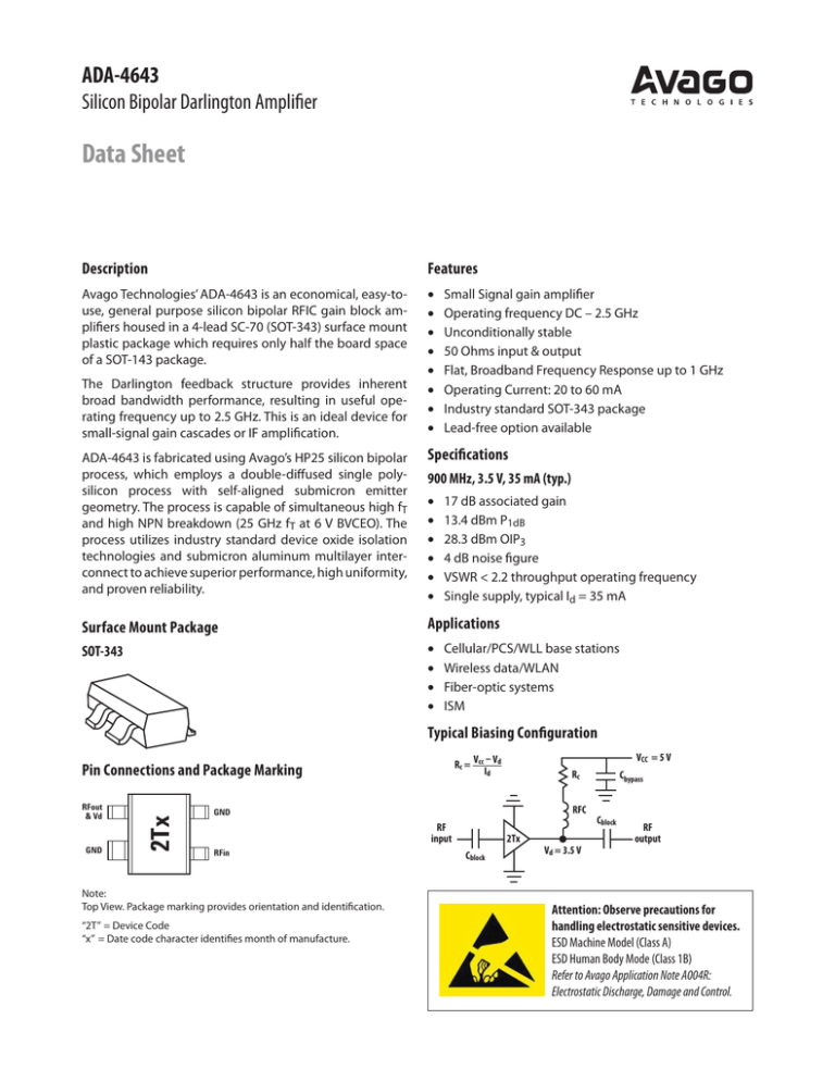
Typical Biasing Configuration
GND
2Tx
RFout
& Vd
VCC = 5 V
Rc = Vcc – Vd
Id
Pin Connections and Package Marking
Rc
RFC
GND
Cblock
RF
input
RFin
Note:
Top View. Package marking provides orientation and identification.
“2T” = Device Code
“x” = Date code character identifies month of manufacture.
Cbypass
2Tx
Cblock
RF
output
Vd = 3.5 V
Attention: Observe precautions for
handling electrostatic sensitive devices.
ESD Machine Model (Class A)
ESD Human Body Mode (Class 1B)
Refer to Avago Application Note A004R:
Electrostatic Discharge, Damage and Control.
ADA-4643 Absolute Maximum Ratings[1]
Absolute
Maximum
Symbol
Parameter
Units
Id
Device Current
mA
70
Pdiss
Total Power Dissipation[2]
mW
270
Pin max.
RF Input Power
dBm
18
Tj
Channel Temperature
C
150
TSTG
Storage Temperature
C
-65 to 150
jc
Thermal Resistance[3]
C/W
152
Notes:
1. Operation of this device above any one of these parameters may cause permanent damage.
2. Ground lead temperature is 25° C. Derate 6.6 mW/°C for TL >109° C.
3. Junction-to-case thermal resistance measured using 150° C Liquid Crystal Measurement method.
ADA-4643 Electrical Specifications
TA = 25° C, Zo = 50 , Pin = -25 dBm, Id = 35 mA (unless specified otherwise)
Symbol
Parameter and Test Condition:
Id = 35 mA, Zo = 50
Vd
Device Voltage Id = 35 mA
Gp
Power Gain (|S21|)2
Gp
Gain Flatness
Frequency
Units
Min.
Typ.
Max.
V
3.2
3.5
3.9
15.5
17.5
17.0
18.5
100 MHz
900 MHz[1,2]
dB
100 to 900 MHz
0.1 to 2 GHz
dB
0.5
1.8
GHz
3.2
F3dB
3 dB Bandwidth
VSWRin
Input Voltage Standing Wave Ratio
0.1 to 6 GHz
2.0:1
VSWRout
Output Voltage Standing Wave Ratio
0.1 to 6 GHz
1.6:1
NF
50 Noise Figure
100 MHz
900 MHz[1,2]
dB
3.9
4.0
P1dB
Output Power at 1dB Gain Compression
100 MHz
900 MHz[1,2]
dBm
14.7
13.4
OIP3
Output 3rd Order Intercept Point
100 MHz[3]
900 MHz[1,2]
dBm
29.0
28.3
DV/dT
Device Voltage Temperature Coefficient
mV/°C
-5.3
Notes:
1. Typical value determined from a sample size of 500 parts from 3 wafers.
2. Measurement obtained using production test board described in the block diagram below.
3. I) 900 MHz OIP3 test condition: F1 = 900 MHz, F2 = 905 MHz and Pin = -25 dBm per tone.
II) 100 MHz OIP3 test condition: F1 = 100 MHz, F2 = 105 MHz and Pin = -25 dBm per tone.
Input
50 Ohm
Transmission
(0.5 dB loss)
DUT
50 Ohm
Transmission
including Bias
(0.5 dB loss)
Block diagram of 900 MHz production test board used for Vd, Gain, P1dB, OIP3, and NF measurements.
Circuit losses have been de-embedded from actual measurements.
2
Output
Std. Dev.
0.07
0.1
Product Consistency Distribution Charts at 900 MHz, Id = 35 mA
300
300
250
250
200
200
150
150
100
100
50
50
0
15
16
17
GAIN (dB)
18
19
Figure 1. Gain distribution @ 35 mA. LSL = 15.5, Nominal = 17, USL = 18.5
0
3
3.2
3.4
3.6
3.8
Vd (V)
Figure 2. Vd distribution @ 35 mA. LSL = 3.2, Nominal = 3.5, USL = 3.9
Notes:
1. Statistics distribution determined from a sample size of 500 parts taken from 3 different wafers.
2. Future wafers allocated to this product may have typical values anywhere between the minimum and maximum specification limits.
3
4
20
20
15
15
P1dB (dBm)
GAIN (dB)
ADA-4643 Typical Performance Curves (at 25° C, unless specified otherwise)
10
10
5
5
0
0
1
2
3
4
FREQUENCY (GHz)
5
0
6
Figure 3. Gain vs. Frequency at Id = 35 mA.
NF (dB)
OIP3 (dBm)
20
15
5
6
5
6
4
3
0
1
2
3
4
FREQUENCY (GHz)
5
2
6
Figure 5. OIP3 vs. Frequency at Id = 35 mA.
0
1
2
3
4
FREQUENCY (GHz)
Figure 6. NF vs. Frequency at Id = 35 mA.
70
18
-40° C
25° C
85° C
60
17
50
16
GAIN (dB)
Id (mA)
3
4
FREQUENCY (GHz)
5
10
40
30
15
14
20
-40° C
25° C
85° C
13
10
0
1
2
3
Vd (V)
Figure 7. Id vs. Vd and Temperature.
4
2
6
25
0
1
Figure 4. P1dB vs. Frequency at Id = 35 mA.
30
5
0
4
5
12
0
10
20
30
40
Id (mA)
Figure 8. Gain vs. Id and Temperature at 900 MHz.
50
60
70
20
35
15
30
10
25
OIP3 (dBm)
P1dB (dBm)
ADA-4643 Typical Performance Curves (at 25° C, unless specified otherwise), continued
5
15
0
-40° C
25° C
85° C
-5
-10
20
0
10
20
30
40
Id (mA)
50
60
5
70
Figure 9. P1dB vs. Id and Temperature at 900 MHz.
5
18
4
16
GAIN (dB)
20
NF (dB)
0
10
20
3
-40° C
25° C
85° C
1
50
0
10
20
30
40
70
4
14
5
50
60
6
10
8
70
Figure 11. NF vs. Id and Temperature at 900 MHz.
0
10
20
30
30
Id (mA)
30
30
40
Figure 12. Gain vs. Id and Frequency (GHz).
25
40
20
5
30
OIP3 (dBm)
10
20
15
-5
10
10
20
30
40
Id (mA)
Figure 13. P1dB vs. Id and Frequency (GHz).
50
60
70
1.5
2.0
2.5
3
25
0
0
0.1
0.5
0.9
35
0.1
0.5
0.9
1.5
2.0
2.5
3
4
5
6
15
-10
60
0.1
0.5
0.9
1.5
2.0
2.5
3
Id (mA)
P1dB (dBm)
40
Id (mA)
12
2
5
30
Figure 10. OIP3 vs. Id and Temperature at 900 MHz.
16
0
-40° C
25° C
85° C
10
5
4
5
6
0
10
20
30
40
Id (mA)
Figure 14. OIP3 vs. Id and Frequency (GHz).
50
60
70
ADA-4643 Typical Performance Curves (at 25° C, unless specified otherwise), continued
6
0
6
5
5.5
-5
4
3
2.5
2.0
1.5
0.9
0.5
0.1
4.5
4
IRL (dB)
NF (dB)
5
Id = 27 mA
Id = 35 mA
Id = 45 mA
Id = 60 mA
-10
-15
3.5
3
0
10
20
30
40
Id (mA)
50
60
70
Figure 15. NF vs. Id and Frequency (GHz).
ORL (dB)
-5
-10
-15
-25
Id = 27 mA
Id = 35 mA
Id = 45 mA
Id = 60 mA
0
2
4
6
8
FREQUENCY (GHz)
Figure 17. Output Return Loss vs. Id and Frequency (GHz).
6
0
2
4
6
8
FREQUENCY (GHz)
Figure 16. Input Return Loss vs. Id and Frequency (GHz).
0
-20
-20
10
12
10
12
ADA-4643 Typical Scattering Parameters, TA = 25° C, Id = 27 mA
Freq.
GHz
S11
S21
Mag.
Ang.
0.1
0.172
1.1
0.5
0.202
10
0.9
0.277
12.3
1.0
0.286
1.5
0.349
1.9
dB
S12
S22
Mag.
Ang.
Mag.
Ang.
Mag.
Ang.
K
17.2
7.246
175.9
0.093
-0.8
0.245
-4.1
1.1
17.04
7.113
160.2
0.091
-4.5
0.245
-12.6
1.1
16.67
6.814
144.7
0.088
-7.4
0.269
-20.4
1.1
9.9
16.56
6.726
141.1
0.087
-7.9
0.274
-23.1
1.1
-2.8
15.98
6.292
124.2
0.083
-9.3
0.28
-37.6
1.1
0.375
-11.3
15.54
5.984
111.4
0.080
-9.5
0.273
-48.9
1.2
2.0
0.382
-13.8
15.44
5.918
108.3
0.080
-9.5
0.271
-51.7
1.2
2.5
0.397
-24.2
14.93
5.581
93.2
0.078
-8.9
0.249
-65.8
1.2
3.0
0.402
-34.7
14.47
5.29
78.6
0.078
-7.8
0.22
-81.7
1.3
3.5
0.394
-46
14.02
5.021
64.2
0.079
-6.6
0.192
-100.9
1.3
4.0
0.378
-58.7
13.58
4.775
50
0.082
-5.4
0.176
-123.8
1.3
4.5
0.361
-73.1
13.16
4.55
35.9
0.087
-4.6
0.179
-148.6
1.3
5.0
0.340
-89.3
12.64
4.284
21.9
0.094
-4.9
0.191
-169.9
1.3
5.5
0.328
-107.1
12.15
4.05
8.3
0.102
-5.9
0.212
173.3
1.2
6.0
0.318
-124.8
11.6
3.803
-5.4
0.112
-8.3
0.233
158.2
1.2
6.5
0.299
-141.1
11.09
3.584
-18.6
0.124
-11.5
0.25
141.6
1.1
7.0
0.274
-159.7
10.56
3.371
-32
0.138
-16.5
0.27
123
1.1
7.5
0.243
177.3
9.96
3.149
-45.6
0.150
-22.8
0.3
103.6
1.1
8.0
0.222
148.7
9.29
2.914
-59.1
0.161
-30
0.337
84.8
1.1
8.5
0.226
119.9
8.41
2.632
-71.8
0.168
-36.7
0.381
70.1
1.1
9.0
0.26
95.4
7.62
2.406
-83.7
0.177
-43
0.429
58.4
1.1
9.5
0.305
75.2
6.67
2.155
-96.1
0.187
-49.9
0.481
48.4
1.1
10.0
0.356
60.1
5.82
1.954
-107.1
0.195
-57.3
0.529
39.7
1
Notes:
1. S-parameters are measured on a microstrip line made on 0.025 inch thick alumina carrier. The input reference plane is at the end of the input lead.
The output reference plane is at the end of the output lead.
7
ADA-4643 Typical Scattering Parameters, TA = 25° C, Id = 35 mA
S11
S21
S12
S22
Freq.
GHz
Mag.
Ang.
0.1
0.151
1.6
17.51
7.504
175.9
0.091
-0.8
0.5
0.185
13.1
17.35
7.367
160.1
0.09
-4.2
0.9
0.265
14.9
16.98
7.06
144.6
0.087
-7
0.251
dB
Mag.
Ang.
Mag.
Ang.
Mag.
Ang.
K
0.223
-4.1
1.1
0.224
-11.7
1.1
-19
1.1
1.0
0.272
12.4
16.86
6.97
140.9
0.086
-7.5
0.256
-21.7
1.1
1.5
0.340
-0.7
16.27
6.511
123.9
0.082
-8.8
0.264
-36.2
1.1
1.9
0.367
-9.5
15.82
6.178
111
0.080
-9.1
0.259
-47.6
1.2
2.0
0.373
-12.1
15.72
6.107
108
0.079
-9.1
0.256
-50.3
1.2
2.5
0.39
-22.7
15.19
5.745
92.8
0.078
-8.5
0.236
-64.4
1.2
3.0
0.395
-33
14.71
5.436
78.3
0.077
-7.3
0.209
-80.4
1.3
3.5
0.387
-44.3
14.23
5.149
63.9
0.079
-6
0.181
-99.9
1.3
4.0
0.370
-57.4
13.79
4.89
49.9
0.082
-4.8
0.166
-123.4
1.3
4.5
0.353
-71.6
13.36
4.657
35.9
0.087
-3.9
0.17
-148.9
1.3
5.0
0.332
-87.7
12.84
4.383
21.9
0.093
-4.2
0.185
-170.6
1.2
5.5
0.319
-106
12.34
4.141
8.3
0.102
-5.1
0.207
172.5
1.2
6.0
0.310
-123.6
11.8
3.889
-5.4
0.112
-7.5
0.23
157.5
1.2
6.5
0.293
-140.2
11.28
3.666
-18.6
0.124
-10.8
0.248
140.9
1.1
7.0
0.266
-158.8
10.75
3.449
-32
0.138
-15.8
0.27
122.3
1.1
7.5
0.238
177.8
10.15
3.219
-45.5
0.151
-22.2
0.301
103
1.1
8.0
0.217
148.5
9.48
2.979
-59
0.161
-29.3
0.34
84.3
1.1
8.5
0.222
119.5
8.62
2.697
-71.7
0.169
-36.1
0.385
69.6
1.1
9.0
0.256
95
7.81
2.458
-83.4
0.178
-42.5
0.434
57.9
1.1
9.5
0.300
74.9
6.88
2.208
-95.8
0.188
-49.5
0.486
47.9
1
10.0
0.357
59.1
6.01
1.996
-107.2
0.196
-56.9
0.534
39.2
1
Notes:
1. S-parameters are measured on a microstrip line made on 0.025 inch thick alumina carrier. The input reference plane is at the end of the input lead.
The output reference plane is at the end of the output lead.
8
ADA-4643 Typical Scattering Parameters, TA = 25° C, Id = 45 mA
S11
S21
S12
S22
Freq.
GHz
Mag.
Ang.
dB
Mag.
Ang.
Mag.
Ang.
Mag.
Ang.
K
0.1
0.137
2.4
17.72
7.691
175.9
0.09
-0.7
0.207
-4
1.1
0.5
0.174
15.3
17.56
7.547
160
0.089
-4
0.209
-10.9
1.1
0.9
0.257
17.4
17.19
7.234
144.5
0.086
-6.8
0.238
-17.6
1.1
1.0
0.267
14.7
17.08
7.144
140.8
0.085
-7.2
0.243
-20.3
1.1
1.5
0.334
0.7
16.47
6.664
123.7
0.081
-8.5
0.253
-34.8
1.1
1.9
0.36
-8.4
16.01
6.317
110.7
0.079
-8.7
0.249
-46.1
1.1
2.0
0.367
-10.9
15.91
6.241
107.7
0.079
-8.7
0.247
-48.9
1.2
2.5
0.386
-21.6
15.36
5.862
92.5
0.077
-8.1
0.227
-62.9
1.2
3.0
0.39
-32.1
14.86
5.534
78
0.077
-7
0.201
-78.9
1.2
3.5
0.382
-43.4
14.38
5.237
63.6
0.078
-5.7
0.174
-98.4
1.3
4.0
0.365
-56.4
13.93
4.971
49.7
0.081
-4.5
0.159
-122.3
1.3
4.5
0.348
-70.8
13.5
4.732
35.7
0.086
-3.6
0.164
-148.3
1.3
5.0
0.327
-86.8
12.97
4.45
21.7
0.093
-3.9
0.179
-170.4
1.2
5.5
0.314
-105.1
12.48
4.205
8.2
0.101
-4.8
0.202
172.6
1.2
6.0
0.304
-122.8
11.93
3.947
-5.5
0.112
-7.1
0.226
157.6
1.2
6.5
0.287
-139.6
11.41
3.721
-18.7
0.124
-10.4
0.245
140.9
1.1
7.0
0.26
-159.1
10.88
3.498
-32
0.138
-15.4
0.268
122.3
1.1
7.5
0.232
177.6
10.28
3.264
-45.6
0.151
-21.8
0.3
102.9
1.1
8.0
0.213
147.8
9.6
3.02
-59.1
0.161
-28.9
0.339
84.2
1.1
8.5
0.218
120.2
8.7
2.724
-71.7
0.169
-35.8
0.385
69.5
1.1
9.0
0.26
94.2
7.95
2.498
-83.7
0.179
-42.1
0.434
57.9
1.1
9.5
0.303
74
6.98
2.233
-96.2
0.189
-49.2
0.487
47.9
1
10.0
0.352
59.4
6.14
2.027
-107.1
0.196
-56.6
0.535
39.1
1
Notes:
1. S-parameters are measured on a microstrip line made on 0.025 inch thick alumina carrier. The input reference plane is at the end of the input lead.
The output reference plane is at the end of the output lead.
9
ADA-4643 Typical Scattering Parameters, TA = 25° C, Id = 60 mA
S11
S21
S12
S22
Freq.
GHz
Mag.
Ang.
0.1
0.126
2.4
17.88
7.834
175.9
0.089
-0.7
0.5
0.165
18.1
17.73
7.696
159.9
0.088
-3.8
0.9
0.252
19.6
17.36
7.377
144.3
0.085
-6.4
0.227
1.0
0.261
16.4
17.24
7.28
140.6
0.085
-6.9
0.233
-18.8
1.1
1.5
0.33
2
16.63
6.787
123.3
0.081
-8.2
0.244
-33.2
1.1
1.9
0.359
-7.4
16.16
6.424
110.3
0.079
-8.4
0.241
-44.4
1.1
2.0
0.365
-9.8
16.05
6.343
107.2
0.078
-8.4
0.239
-47.2
1.1
2.5
0.386
-21
15.49
5.948
91.9
0.077
-7.8
0.221
-61
1.2
3.0
0.387
-31.5
14.98
5.61
77.4
0.077
-6.7
0.195
-76.8
1.2
3.5
0.381
-43
14.49
5.301
63.1
0.078
-5.5
0.168
-96.2
1.3
4.0
0.363
-56
14.02
5.025
49
0.081
-4.3
0.153
-120.3
1.3
4.5
0.344
-70.7
13.58
4.777
35
0.086
-3.5
0.157
-146.9
1.3
5.0
0.323
-87.3
13.04
4.488
21
0.093
-3.7
0.172
-169.4
1.2
5.5
0.31
-105.8
12.54
4.235
7.5
0.101
-4.6
0.195
173.4
1.2
6.0
0.301
-123.6
11.98
3.971
-6.2
0.111
-6.9
0.22
158.2
1.2
6.5
0.281
-140.6
11.44
3.735
-19.4
0.124
-10.2
0.239
141.4
1.1
7.0
0.257
-159.9
10.9
3.507
-32.7
0.138
-15.2
0.262
122.5
1.1
7.5
0.228
176.3
10.29
3.271
-46.3
0.151
-21.5
0.294
103
1.1
8.0
0.212
145.6
9.61
3.022
-59.8
0.161
-28.6
0.333
84.3
1.1
8.5
0.218
117.8
8.72
2.728
-72.4
0.169
-35.6
0.38
69.5
1.1
9.0
0.257
92.7
7.94
2.494
-84.1
0.178
-41.8
0.429
57.9
1.1
9.5
0.302
72.9
6.98
2.234
-96.4
0.189
-48.9
0.482
47.9
1
10.0
0.359
57.7
6.11
2.02
-107.7
0.196
-56.4
0.531
39.2
1
dB
Mag.
Ang.
Mag.
Ang.
Mag.
Ang.
K
0.194
-3.8
1.1
0.196
-9.9
1.1
-16.1
1.1
Notes:
1. S-parameters are measured on a microstrip line made on 0.025 inch thick alumina carrier. The input reference plane is at the end of the input lead.
The output reference plane is at the end of the output lead.
10
Ordering Information
Part Number
No. of Devices
Container
ADA-4643-TR1
3000
7” Reel
ADA-4643-TR2
10000
13” Reel
ADA-4643-BLK
100
antistatic bag
ADA-4643-TR1G
3000
7” Reel
ADA-4643-TR2G
10000
13” Reel
ADA-4643-BLKG
100
antistatic bag
Note: For lead-free option, the part number will have the character “G” at the end.
Package Dimensions
Recommended PCB Pad Layout for
Avago’s SC70 4L/SOT-343 Products
Outline 43
SOT-343 (SC70 4-lead)
1.30
(0.051)
1.30 (.051)
BSC
1.00
(0.039)
HE
E
2.00
(0.079)
0.60
(0.024)
1.15 (.045) BSC
0.9
(0.035)
b1
1.15
(0.045)
D
Dimensions in
A2
A
A1
b
L
C
DIMENSIONS (mm)
SYMBOL
E
D
HE
A
A2
A1
b
b1
c
L
11
MIN.
1.15
1.85
1.80
0.80
0.80
0.00
0.15
0.55
0.10
0.10
MAX.
1.35
2.25
2.40
1.10
1.00
0.10
0.40
0.70
0.20
0.46
NOTES:
1. All dimensions are in mm.
2. Dimensions are inclusive of plating.
3. Dimensions are exclusive of mold flash & metal burr.
4. All specifications comply to EIAJ SC70.
5. Die is facing up for mold and facing down for trim/form,
ie: reverse trim/form.
6. Package surface to be mirror finish.
mm
(inches)
Device Orientation
REEL
TOP VIEW
END VIEW
4 mm
CARRIER
TAPE
8 mm
USER
FEED
DIRECTION
COVER TAPE
Tape Dimensions
For Outline 4T
P
P2
D
P0
E
F
W
C
D1
t1 (CARRIER TAPE THICKNESS)
Tt (COVER TAPE THICKNESS)
K0
10° MAX.
A0
DESCRIPTION
10° MAX.
B0
SYMBOL
SIZE (mm)
SIZE (INCHES)
CAVITY
LENGTH
WIDTH
DEPTH
PITCH
BOTTOM HOLE DIAMETER
A0
B0
K0
P
D1
2.40 ± 0.10
2.40 ± 0.10
1.20 ± 0.10
4.00 ± 0.10
1.00 + 0.25
0.094 ± 0.004
0.094 ± 0.004
0.047 ± 0.004
0.157 ± 0.004
0.039 + 0.010
PERFORATION
DIAMETER
PITCH
POSITION
D
P0
E
1.50 ± 0.10
4.00 ± 0.10
1.75 ± 0.10
0.061 + 0.002
0.157 ± 0.004
0.069 ± 0.004
CARRIER TAPE
WIDTH
THICKNESS
W
t1
8.00 + 0.30 - 0.10
0.254 ± 0.02
0.315 + 0.012
0.0100 ± 0.0008
COVER TAPE
WIDTH
TAPE THICKNESS
C
Tt
5.40 ± 0.10
0.062 ± 0.001
0.205 + 0.004
0.0025 ± 0.0004
DISTANCE
CAVITY TO PERFORATION
(WIDTH DIRECTION)
F
3.50 ± 0.05
0.138 ± 0.002
CAVITY TO PERFORATION
(LENGTH DIRECTION)
P2
2.00 ± 0.05
0.079 ± 0.002
For product information and a complete list of distributors, please go to our web site:
www.avagotech.com
Avago, Avago Technologies, and the A logo are trademarks of Avago Technologies in the United States and other countries.
Data subject to change. Copyright © 2005-2012 Avago Technologies. All rights reserved. Obsoletes 5989-3753EN
AV02-3598EN - June 8, 2012
