ADA-4789
Silicon Bipolar Darlington Amplifier
Data Sheet
Description
Features
Avago Technologies’ ADA-4789 is an economical, easyto-use, general purpose silicon bipolar RFIC gain block
amplifiers housed in SOT-89 surface mount plastic
package.
•
•
•
•
•
•
•
•
•
The Darlington feedback structure provides inherent
broad bandwidth performance, resulting in useful
operating frequency up to 2.5 GHz. This is an ideal
device for small-signal gain cascades or IF amplification.
ADA-4789 is fabricated using Avago’s HP25 silicon
bipolar process, which employs a double-diffused
single poly-silicon process with self-aligned submicron
emitter geometry. The process is capable of
simultaneous high fT and high NPN breakdown (25 GHz
fT at 6V BVCEO). The process utilizes industry standard
device oxide isolation technologies and submicron
aluminum multi-layer inter-connects to achieve
superior performance, high uniformity, and proven
reliability.
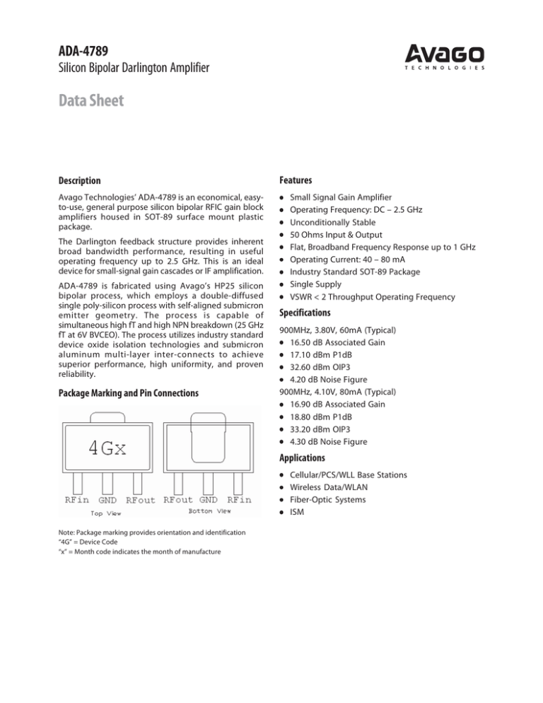
Package Marking and Pin Connections
Small Signal Gain Amplifier
Operating Frequency: DC – 2.5 GHz
Unconditionally Stable
50 Ohms Input & Output
Flat, Broadband Frequency Response up to 1 GHz
Operating Current: 40 – 80 mA
Industry Standard SOT-89 Package
Single Supply
VSWR < 2 Throughput Operating Frequency
Specifications
900MHz, 3.80V, 60mA (Typical)
• 16.50 dB Associated Gain
• 17.10 dBm P1dB
• 32.60 dBm OIP3
• 4.20 dB Noise Figure
900MHz, 4.10V, 80mA (Typical)
• 16.90 dB Associated Gain
• 18.80 dBm P1dB
• 33.20 dBm OIP3
• 4.30 dB Noise Figure
Applications
•
•
•
•
Note: Package marking provides orientation and identification
“4G” = Device Code
“x” = Month code indicates the month of manufacture
Cellular/PCS/WLL Base Stations
Wireless Data/WLAN
Fiber-Optic Systems
ISM
Table 1. Absolute Maximum Ratings [1] at Tc = +25°C
Typical Biasing Configuration
VCC = 5 V
V -V
Rc = cc d
Id
Rc
C bypass
RFC
C block
RF
input
3Tx
Vd = 3.8 V
C block
RF
output
Symbol Parameter
Unit
Max
Rating
Id
Device Current
mA
90
Pdiss
Total Power Dissipation[2]
mW
370
Pin max
RF Input Power
dBm
20
Tj
Junction Temperature
0
C
150
Storage Temperature
0
C
-65 to 150
[3]
0
C/W
50
Tstg
θjc
Thermal Resistance
Notes:
1. Operation in excess of any one of these conditions may result in
permanent damage to the device.
2. Ground lead temperature is 25°C. Derate 20 mW/°C for Tc > 131.5
°C.
3. Thermal Resistance is measured from junction to board using IR
method.
Table 2. Electrical Specifications at Tc = +25°C
Symbol
Parameter and Test Condition:
Id = 60mA, Zo = 50Ω
Vd
Device Voltage
Gp
Power Gain
Frequency
Units
V
100 MHz
900 MHz [1,2]
2.0 GHz
100 to 900 MHz
0.1 to 2.0 GHz
Min.
3.3
dB
15
Max.
3.8
4.3
16.9
16.5
16.2
0.3
0.5
4
Gp
Gain Flatness
F3dB
3dB Bandwidth
VSWRin
Input Voltage Standing Wave Ratio
0.1 to 4.0 GHz
1.3:1
VSWRout
Output Voltage Standing Wave Ratio
0.1 to 4.0 GHz
1.5:1
NF
50Ω Noise Figure
P1dB
Output Power at 1dB Gain Compression
100 MHz
900 MHz [1,2]
2.0 GHz
100 MHz
900 MHz [1,2]
2.0 GHz
100 MHz [3]
900 MHz [1,2,3]
2.0 GHz [3]
OIP3
dV/dT
Output Third Order Intercept Point
GHz
Device Voltage Temperature Coefficient
Notes:
1. Typical value determined from a sample size of 500 parts from 3 wafers.
2. Measurement obtained using production test board described in the block diagram below.
3. i) 100 MHz OIP3 Test Condition: F1 = 100 MHz, F2 = 105 MHz, Pin = -20 dBm per tone.
ii)900 MHz OIP3 Test Condition: F1 = 900 MHz, F2 = 905 MHz, Pin = -20 dBm per tone.
iii) 2000 MHz OIP3 Test Condition: F1 = 2000 MHz, F2 = 2005 MHz, Pin = -20 dBm per tone.
2
dB
Typ.
dB
dBm
16.0
dBm
27
mV/0C
4.1
4.2
4.4
17.7
17.1
16.2
33.4
32.6
28.8
-4.9
18
Table 3. Typical Electrical performance at Tc = +25°C, Id=80mA, Zo= 50 Ω
Symbol
Parameter and Test Condition:
Vd
Device Voltage
Gp
Power Gain
NF
50Ω Noise Figure
P1dB
Output Power at 1dB Gain Compression
OIP3
Output Third Order Intercept Point
Frequency
100 MHz
900 MHz [1,2]
2.0 GHz
100 MHz
900 MHz [1,2]
2.0 GHz
100 MHz
900 MHz [1,2]
2.0 GHz
100 MHz [3]
900 MHz [1,2,3]
2.0 GHz [3]
Units
Min.
Typ.
V
4.1
dB
17.1
16.9
16.3
4.1
4.3
4.5
19.3
18.8
16.9
35.4
33.2
29
dB
dBm
dBm
Max.
Notes:
1. Typical value determined from a sample size of 200 parts from 2 wafers.
2. Measurement obtained using production test board described in the block diagram below.
3 i) 100 MHz OIP3 Test Condition: F1 = 100 MHz, F2 = 105 MHz, Pin = -20 dBm per tone.
ii) 900 MHz OIP3 Test Condition: F1 = 900 MHz, F2 = 905 MHz, Pin = -20 dBm per tone.
iii) 2000 MHz OIP3 Test Condition: F1 = 2000 MHz, F2 = 2005 MHz, Pin = -20 dBm per tone.
Block Diagram
Input
50 Ohm
Transmission
(0.5 dB loss)
DUT
50 Ohm
Transmission
including Bias
(0.5 dB loss)
Output
Block diagram of 900 MHz production test board used for Vd, Gain, P1dB, OIP3, and NF measurements show in
table 2 & 3. Circuit losses have been de-embedded from actual measurement.
3
Product Consistency Distribution Charts at 900 MHz, Id=60mA
Figure 1. Vd Distribution@60mA.
Figure 2. Gain Distribution@60mA.
LSL=3.3V, Nominal=3.8V, USL=4.3V
LSL=15 dB, Nominal=16.5 dB, USL=18 dB
Figure 3. P1dB Distribution@60mA
Figure 4. OIP3 Distribution@60mA.
LSL=16.0 dBm, Nominal=17.1dBm
LSL=27 dBm, Nominal=32.6 dBm
Notes:
1. Statistics distribution determined from a sample size of 500 parts taken from 3 different wafers.
2. Future wafers allocated to this product may have typical values anywhere between the minimum and maximum specification limits.
20
20
15
15
P1dB (dBm)
Gain (dB)
Typical Performance Curve (at Tc=25°C, unless specified otherwise)
10
5
5
0
0
0
1
2
3
4
Frequency (GHz)
Figure 5. Gain vs Frequency at Id = 60 mA.
4
10
5
6
0
1
2
3
4
Frequency (GHz)
Figure 6. P1dB vs Frequency at Id = 60 mA.
5
6
6
35
5
NF (dB)
OIP3 (dBm)
30
25
4
20
3
15
2
10
0
1
2
3
4
5
0
6
Frequency (GHz)
Figure 7. OIP3 vs Frequency at Id = 60 mA.
2
3
4
5
6
Frequency (GHz)
Figure 8. NF vs Frequency at Id = 60 mA.
90
17.0
80
-40C
25C
85C
70
16.5
60
16.0
Gain (dB)
Id (mA)
1
50
40
30
15.5
15.0
20
-40C
25C
85C
14.5
10
0
0
1
2
3
4
14.0
5
0
20
Vd (V)
40
60
80
100
Id (mA)
Figure 9. Id vs. Vd and Temperature.
Figure 10. Gain vs. Id and Temperature at 900 MHz.
20
40
18
35
16
30
OIP3 (dBm)
P1dB (dB)
14
12
10
8
25
20
15
6
2
0
0
0.02
0.04
0.06
0.08
Id (mA)
Figure 11. P1dB vs. Id and Temperature at 900 MHz.
5
10
-40C
25C
85C
4
-40C
25C
85C
5
0.1
0
0
20
40
60
80
Id (mA)
Figure 12. OIP3 vs. Id and Temperature at 900 MHz.
100
18
6
0.1
0.9
1.5
2
3
4
17
5
16
15
Gain (dB)
NF (dB)
4
3
14
5
13
12
2
11
-40C
25C
85C
1
6
10
9
0
0
20
40
60
80
0
100
20
40
60
80
Id (mA)
Id (mA)
Figure 13. NF vs. Id and Temperature at 900 MHz.
20
Figure 14. Gain vs Id and Frequency (GHz).
40
0.1
0.9
1.5
2
35
3
30
0.1
0.9
10
OIP3 (dBm)
P1dB (dBm)
15
4
5
5
6
1.5
2
25
3
20
4
5
15
6
10
0
0
20
40
100
60
80
100
0
20
40
60
80
100
Id (mA)
Id (mA)
Figure 15. P1dB vs Id and Frequency (GHz).
Figure 16. OIP3 vs Id and Frequency (GHz).
6
0
6
5.5
-5
5
IRL (dB)
NF (dB)
5
4
3
2
1.5
0.9
0.1
4.5
4
20
40
60
Id (mA)
Figure 17. NF vs Id and Frequency (GHz).
6
80
-15
Id=50mA
Id=60mA
Id=80mA
-20
3.5
0
-10
100
-25
0
2
4
6
8
10
FREQUENCY (GHz)
Figure 18. Input Return Loss vs Id and Frequency.
12
0
20
-5
-10
Gain (dB)
ORL (dB)
15
-15
Id=50mA
Id=60mA
Id=80mA
-20
10
5
-25
0
0
2
4
6
8
10
12
0
1
FREQUENCY (GHz)
2
3
4
5
6
Frequency (GHz)
Figure 19. Output Return Loss vs Id and Frequency.
Figure 20. Gain vs Frequency at Id = 80 mA
40
20
35
OIP3 (dBm)
P1dB (dBm)
15
10
30
25
20
5
15
10
0
0
1
2
3
4
5
6
Frequency (GHz)
NF (dB)
5
4
3
2
2
3
4
Frequency (GHz)
Figure 23. NF vs Frequency at Id = 80 mA
7
2
3
Figure 22. OIP3 vs Frequency at Id = 80 mA
6
1
1
4
Frequency (GHz)
Figure 21. P1dB vs Frequency at Id = 80 mA
0
0
5
6
5
6
Typical Scattering Parameters At 25°C, Id = 50mA
S11
S21
Mag.
Ang.
Mag.
S22
Mag.
Ang.
0.1
0.168
3.0
16.469
6.660
171.3
0.099
-0.2
0.168
-8.4
0.5
0.110
-12.5
16.213
6.466
164.0
0.098
-7.0
0.188
-28.0
0.9
0.087
-50.0
16.182
6.443
144.7
0.094
-14.4
0.157
-72.9
1.0
0.083
-60.1
16.172
6.436
140.0
0.092
-19.2
0149
-84.4
1.9
0.093
-155.0
15.741
6.124
107.1
0.085
-26.3
0.218
-110.7
2.0
0.103
-144.8
15695
6.092
103.4
0.084
-27.1
0.226
-114.1
2.5
0.095
176.1
15.528
5.976
84.8
0.084
-31.3
0.292
-146.6
Freq. GHz
dB
S12
Ang.
Mag.
Ang.
3.0
0.114
144.7
15.362
5.863
66.0
0.085
-35.4
0.358
181.0
3.5
0.154
123.7
15.199
5.754
47.4
0.087
-39.4
0.422
149.3
4.0
0.196
106.1
15.035
5.646
28.7
0.088
-43.6
0.486
115.4
4.5
0.246
98.3
14.357
5.222
9.2
0.086
-49.3
0.559
100.4
5.0
0.344
85.8
13.120
4.529
-11.0
0.084
-56.4
06.29
87.6
5.5
0.405
74.7
11.925
3.947
-31.4
0.083
-64.8
0.669
73.2
6.0
0.489
61.4
10.243
3.252
-50.4
0.080
-72.9
0.700
59.1
6.5
0.540
52.2
9.030
2.828
-67.1
0.076
-79.7
0.732
47.9
7.0
0.582
44.3
7.854
2.470
-82.5
0.071
-86.8
0.764
37.3
7.5
0.625
36.5
6.477
2.108
-97.9
0.067
-93.6
0.794
26.6
8.0
0.667
28.5
4.851
1.748
-113.2
0.061
-100.6
0.827
16.0
8.5
0.696
23.7
3.027
1.417
-122.2
0.055
-104.6
0.827
12.5
9.0
0.728
18.8
0.725
1.087
228.9
0.049
251.6
0.826
9.2
9.5
0.737
13.2
-0.715
0.921
221.1
0.046
245.4
0.816
6.2
10.0
0.738
9.9
-1.809
0.812
-148.1
0.045
238.0
0.797
1.8
Notes:
S parameters are measured on a micro-strip line made on 0.025 inch thick alumina carrier. The input reference plane is at the end of the RFin
lead. The output reference plane is at the end of the RFout lead.
8
Typical Scattering Parameters At 25°C, Id = 60mA
S11
S21
S12
S22
Freq. GHz
Mag.
Ang.
dB
Mag.
Ang.
Mag.
Ang.
Mag.
Ang.
0.1
0.160
3.1
16.586
6.750
171.3
0.099
-0.2
0.160
-8.5
0.5
0.110
-6.1
16.325
6.550
164.1
0.098
-6.9
0.180
-30.7
0.9
0.087
-44.2
16.292
6.525
144.8
0.093
-14.2
0.150
-75.4
1.0
0.081
-54.5
16.284
6.519
140.0
0.092
-19.1
0.143
-86.6
1.9
0.089
-151.3
15.855
6.205
107.1
0.084
-26.3
0.212
-112.3
2.0
0.097
-142.1
15.806
6.170
103.4
0.083
-27.1
0.220
-115.2
2.5
0.090
178.3
15.639
6.053
84.7
0.084
-31.2
0.287
-147.7
3.0
0.109
146.7
15.471
5.937
66.0
0.085
-35.3
0.353
179.8
3.5
0.149
126.8
15.298
5.820
47.4
0.086
-39.3
0.420
147.3
4.0
0.198
110.5
15.122
5.703
28.7
0.087
-43.4
0.487
114.7
4.5
0.253
97.5
14.441
5.273
9.3
0.085
-49.1
0.560
100.2
5.0
0.350
85.3
13.217
4.580
-10.9
0.083
-56.2
0.630
87.5
5.5
0.410
74.5
12.019
3.990
-31.3
0.082
-64.6
0.670
73.2
6.0
0.493
61.0
10.344
3.290
-50.2
0.080
-72.3
0.703
59.2
6.5
0.544
52.0
9.124
2.859
-66.9
0.075
-79.3
0.735
47.9
7.0
0.586
44.1
7.945
2.496
-82.3
0.070
-86.2
0.767
37.3
7.5
0.628
36.2
6.580
2.133
-97.6
0.066
-93.1
0.798
26.6
8.0
0.670
28.3
4.959
1.770
-113.0
0.061
-100.0
0.830
16.0
8.5
0.700
23.5
3.317
1.435
-122.0
0.055
-104.0
0.830
12.6
9.0
0.730
18.6
0.828
1.100
229.1
0.049
252.0
0.830
9.2
9.5
0.740
13.1
-0.630
0.930
221.4
0.046
246.0
0.820
6.2
10.0
0.740
9.7
-1.724
0.820
-147.8
0.045
238.6
0.800
1.7
Notes:
S parameters are measured on a micro-strip line made on 0.025 inch thick alumina carrier. The input reference plane is at the end of the RFin
lead. The output reference plane is at the end of the RFout lead.
9
Typical Scattering Parameters At 25°C, Id = 80mA
S11
S21
S12
S22
Freq. GHz
Mag.
Ang.
dB
Mag.
Ang.
Mag.
Ang.
Mag.
Ang.
0.1
0.151
3.1
16.716
6.852
171.3
0.098
-0.2
0.150
-8.5
0.5
0.112
1.1
16.45
6.645
164.1
0.097
-6.8
0.171
-34.4
0.9
0.087
-37.7
16.416
6.619
144.7
0.092
-14.2
0.142
-78.4
1.0
0.081
-48.0
16.408
6.613
140.0
0.091
-18.9
0.135
-89.3
1.9
0.086
-147.0
15.980
6.295
107.0
0.084
-26.1
0.204
-114.1
2.0
0.093
-138.8
15.931
6.260
103.3
0.083
-27.0
0.212
-116.3
2.5
0.085
181.0
15.768
6.143
84.6
0.083
-31.0
0.279
-148.7
3.0
0.104
148.5
15.596
6.023
65.8
0.084
-35.1
0.347
178.6
3.5
0.145
129.5
15.414
5.898
47.2
0.085
-39.2
0.417
144.7
4.0
0.199
114.6
15.227
5.772
28.5
0.086
-43.2
0.487
113.6
4.5
0.259
98.5
14.543
5.335
9.0
0.084
-48.8
0.562
99.6
5.0
0.356
85.3
13.319
4.634
-11.2
0.083
-55.9
0.630
87.1
5.5
0.417
74.4
12.108
4.031
-31.6
0.081
-64.1
0.670
73.0
6.0
0.500
60.9
10.428
3.322
-50.6
0.079
-72.1
0.702
59.0
6.5
0.551
51.8
9.191
2.881
-67.2
0.075
-78.7
0.735
47.8
7.0
0.592
43.9
8.000
2.512
-82.6
0.070
-85.6
0.767
37.1
7.5
0.634
36.0
6.629
2.145
-97.9
0.066
-92.6
0.798
26.5
8.0
0.674
28.0
4.994
1.777
-113.2
0.060
-99.6
0.830
15.9
8.5
0.705
23.3
3.161
1.439
-122.1
0.054
-103.5
0.830
12.5
9.0
0.733
18.4
0.844
1.102
229.0
0.049
252.9
0.830
9.1
9.5
0.743
12.9
-.0.602
0.933
221.4
0.046
-113.4
0.820
6.2
10.0
0.744
9.6
-1.713
0.821
-147.7
0.045
239.1
0.800
1.6
Notes:
S parameters are measured on a micro-strip line made on 0.025 inch thick alumina carrier. The input reference plane is at the end of the RFin
lead. The output reference plane is at the end of the RFout lead.
10
Part Number Ordering Information
Part Number
No of Devices Container
ADA-4789-TR1G
3000
13" Reel
ADA-4789-BLKG
100
Anti-Static Bag
SOT 89 Package Dimensions
Notes:
1. Dimensioning and tolerancing per
ANSI.Y14.5M-1982
2. Controlling dimension: Milimeter
convert to Inch are not necessary exact.
3. Dimension B1, 2 places.
11
Device Orientation
Tape Dimensions
For product information and a complete list of distributors, please go to our web site:
www.avagotech.com
Avago, Avago Technologies, and the A logo are trademarks of Avago Technologies, Limited in the United States and other countries.
Data subject to change. Copyright © 2007 Avago Technologies Limited. All rights reserved. Obsoletes AV01-0295EN
AV02-0052EN - January 12, 2007
