AN-1412
APPLICATION NOTE
One Technology Way • P.O. Box 9106 • Norwood, MA 02062-9106, U.S.A. • Tel: 781.329.4700 • Fax: 781.461.3113 • www.analog.com
4 mA to 20 mA Process Control Loop Using the AD5662 DAC
CIRCUIT FUNCTION AND BENEFITS
with 16-bit resolution and monotonicity, which is powered
directly from the 4 mA to 20 mA control loop power supply and
consumes less than 4 mA. Transmitters requiring more than
4 mA cannot be powered directly from the loop power supply
and, therefore, require an additional supply.
In many process control applications, 2-wire current transmitters
are often used to transmit analog signals through noisy environments. These current transmitters use a zero-scale signal current of
4 mA and a full-scale signal current of 20 mA—therefore the
designation: 4 mA to 20 mA converter. The circuit described in
this application note provides a low power current transmitter
+
C2
0.1µF
VOUT
5V
C3
10µF
+
C5
0.1µF
C4
0.1µF
R2
1MΩ
SYNC
SCLK
VDD
VFB
AD5662
DIN
GND
PCB GROUND
C6
10µF
VREF
+
EXTERNAL
LOOP
SUPPLY
7V TO 36V
+
C1
10µF
VOUT
R1
200kΩ
R3
69.8kΩ
AD8627
R4
1.2kΩ
R5
3.3kΩ
D1
4mA TO 20mA
C7
390pF
RL
RS
100Ω
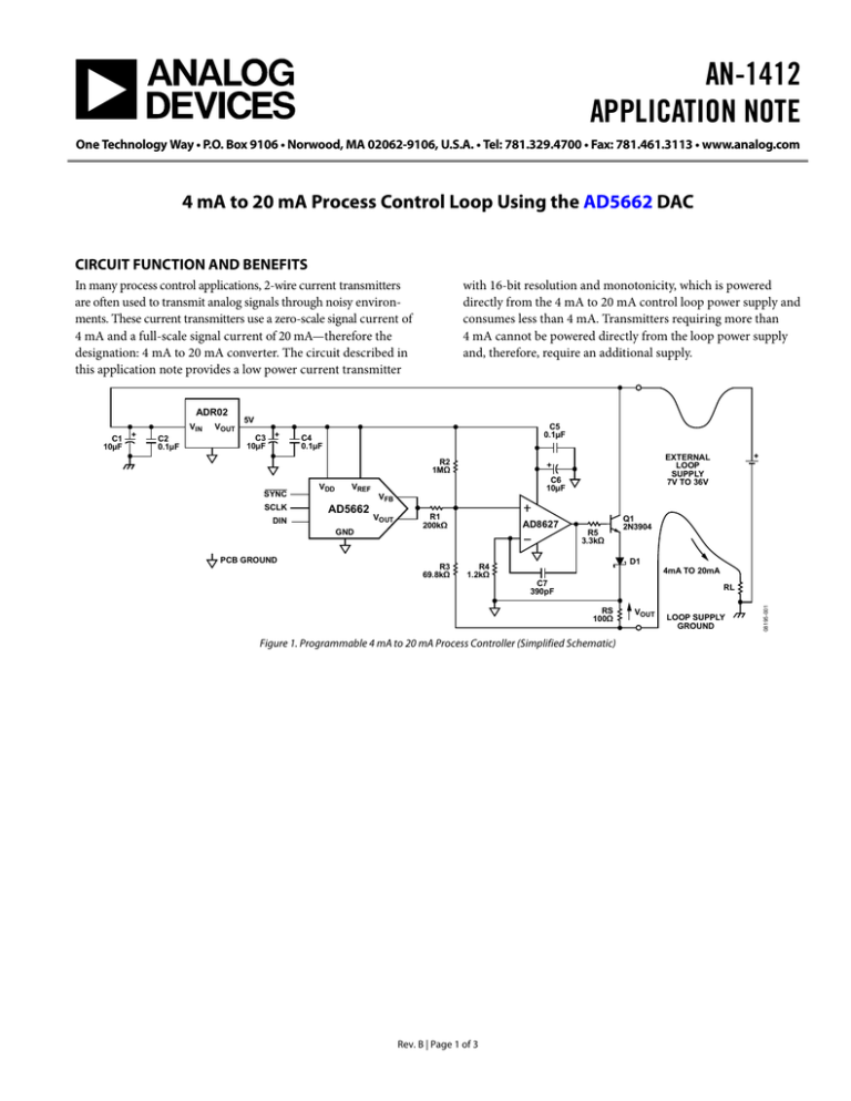
Figure 1. Programmable 4 mA to 20 mA Process Controller (Simplified Schematic)
Rev. B | Page 1 of 3
Q1
2N3904
VOUT
LOOP SUPPLY
GROUND
08195-001
ADR02
VIN
AN-1412
Application Note
TABLE OF CONTENTS
Circuit Function and Benefits ......................................................... 1
Common Variations ..........................................................................3
Revision History ............................................................................... 2
Reference ............................................................................................3
Circuit Description ........................................................................... 3
REVISION HISTORY
7/2016—Rev. A to Rev. B
Document Title Changed from CN-0009 to AN-1412 ...... Universal
5/2009—Rev. 0 to Rev. A
Updated Format .......................................................................... Universal
10/2008—Revision 0: Initial Version
Rev. B | Page 2 of 3
Application Note
AN-1412
For the values shown in Figure 1,
CIRCUIT DESCRIPTION
This circuit provides a programmable output current of 4 mA to
20 mA using the AD5662 nanoDAC® converter as a controller.
The loop current is sensed by measuring the voltage, VOUT,
which is dropped across RS. If the digital-to-analog converter
(DAC) output is 0 V, a current of
5V
VREF
=
= 5 µA
R2 1 MΩ
(1)
flows through R2 and R3, forcing the printed circuit board
(PCB) ground to be 349 mV more positive than the voltage
measured at the load side of RS. The RS voltage of 349 mV
corresponds to a loop current of
VOUT 349 mV
=
= 3.49 mA
RS
100 Ω
(2)
When the DAC outputs a full-scale voltage of 5 V, the current
through R2 is
5V
VREF
=
= 5 µA
R2 1 MΩ
(3)
The current through R1 is
5V
VREF
=
= 25 µA
R1
200 kΩ
(4)
Therefore, the current through R3 is
VREF VREF
+
= 5 µA + 25 µA = 30 µA
R2
R1
(5)
The R3 current forces the voltage, VOUT, across RS to equal
30 µA × 69.8 kΩ = 2.09 V
(6)
The feedback loop around the AD8627 forces the voltage at its
noninverting input to equal the PCB ground voltage. The
output current is, therefore, directly proportional to the digital
code. The AD8627 regulates the DAC output current to satisfy
the current summation at its noninverting node. The output
current is calculated using the following equation:
I OUT =
R3
R3
1
VDAC ×
+ VREF ×
R1
R2
RS
IOUT = (0.266 µA × D) +3.49 mA
(8)
where 0 ≤ D ≤ 65,535. D represents the input code in decimals.
This circuit gives a full-scale output current of 20.9 mA when
the AD5662 digital code equals 0xFFFF. Likewise, the output
current of the AD5662 is 3.49 mA when the digital code equals
0x0000. The extended current range (3.49 mA to 20.9 mA)
allows the user to calibrate the 4 mA to 20 mA range by using
software and the 16-bit resolution of the AD5662. The Schottky
diode is required in this circuit to prevent loop supply power-on
transients from pulling the noninverting input of the AD8627
more than 300 mV below its inverting input. The Schottky diode
must be able to handle at least the 20 mA full loop load.
Biasing for the controller is provided by the ADR02 precision
5 V reference, and the circuit requires no external trims because
of the tight initial output voltage tolerance of the ADR02 and
the low supply current of both the AD8627 and the AD5662.
The limits on the allowable loop power supply are set by the
ADR02 minimum input voltage (7 V) and maximum input
voltage (36 V). The 2N3904 (Q1 in Figure 1) maximum
allowable power dissipation at 25°C is 625 mW; therefore a
higher power transistor must be used if the loop supply exceeds
about 30 V. Power dissipation in the 2N3904 can be reduced by
adding an appropriate voltage dropping resistor in series with
its collector.
COMMON VARIATIONS
The basic circuit is flexible and can accommodate a number of
different references, voltage output DACs, and op amps.
Considerations are reference accuracy, DAC resolution, and
amplifier offset voltage. The prime requirement is that the total
circuit must operate on the loop supply voltage and require less
than 4 mA of quiescent current (for a DAC code of 0x0000).
REFERENCE
Voltage Reference Wizard Design Tool
(7)
©2008–2016 Analog Devices, Inc. All rights reserved. Trademarks and
registered trademarks are the property of their respective owners.
AN08195-0-7/16(B)
Rev. B | Page 3 of 3


