Lecture 17 - EECS Instructional Support Group Home Page
advertisement
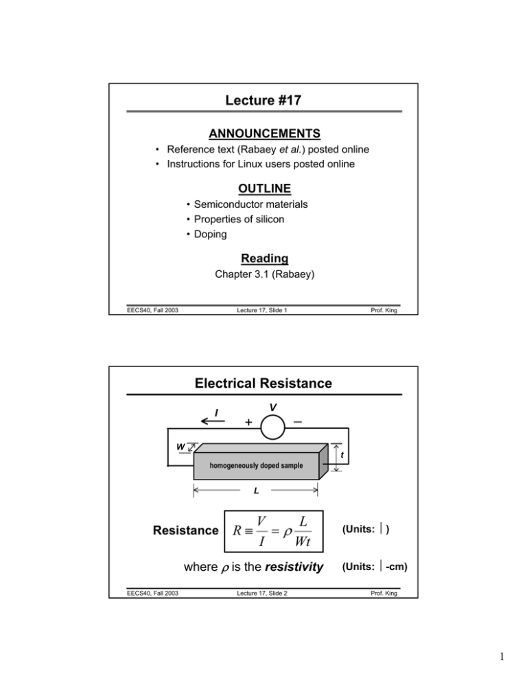
Lecture #17 ANNOUNCEMENTS • Reference text (Rabaey et al.) posted online • Instructions for Linux users posted online OUTLINE • Semiconductor materials • Properties of silicon • Doping Reading Chapter 3.1 (Rabaey) EECS40, Fall 2003 Lecture 17, Slide 1 Prof. King Electrical Resistance I V + _ W t homogeneously doped sample L Resistance R≡ V L =ρ I Wt where ρ is the resistivity EECS40, Fall 2003 Lecture 17, Slide 2 (Units: Ω) (Units: Ω-cm) Prof. King 1 What is a Semiconductor? • Low resistivity => “conductor” • High resistivity => “insulator” • Intermediate resistivity => “semiconductor” – Generally, the semiconductor material used in integrated-circuit devices is crystalline • In recent years, however, non-crystalline semiconductors have become commercially very important polycrystalline EECS40, Fall 2003 amorphous crystalline Lecture 17, Slide 3 Prof. King Semiconductor Materials Elemental: Compound: Alloy: EECS40, Fall 2003 Lecture 17, Slide 4 Prof. King 2 The Silicon Atom • 14 electrons occupying the 1st 3 energy levels: – 1s, 2s, 2p orbitals filled by 10 electrons – 3s, 3p orbitals filled by 4 electrons To minimize the overall energy, the 3s and 3p orbitals hybridize to form 4 tetrahedral 3sp orbitals Each has one electron and is capable of forming a bond with a neighboring atom EECS40, Fall 2003 Lecture 17, Slide 5 Prof. King The Si Crystal “diamond cubic” lattice • Each Si atom has 4 nearest neighbors • lattice constant = 5.431Å EECS40, Fall 2003 Lecture 17, Slide 6 Prof. King 3 Compound Semiconductors Ga As • “zinc blende” structure • III-V compound semiconductors: GaAs, GaP, GaN, etc. 9 important for optoelectronics and high-speed ICs EECS40, Fall 2003 Lecture 17, Slide 7 Prof. King Electronic Properties of Si • Silicon is a semiconductor material. Pure Si has relatively high resistivity at room temperature. • There are 2 types of mobile charge-carriers in Si: Conduction electrons are negatively charged. Holes are positively charged. • The concentration of conduction electrons & holes in a semiconductor can be affected in several ways: 1. 2. 3. 4. by adding special impurity atoms (dopants) by applying an electric field by changing the temperature by irradiation EECS40, Fall 2003 Lecture 17, Slide 8 Prof. King 4 Conduction Electrons and Holes 2-D representation When an electron breaks loose and becomes a conduction electron, a hole is also created. Si Si Si Si Si Si Si Si Si Note: A hole (along with its associated positive charge) is mobile! EECS40, Fall 2003 Lecture 17, Slide 9 Prof. King Definition of Parameters n = number of electrons per cm3 p = number of holes per cm3 ni = intrinsic carrier concentration (#/cm3) In a pure semiconductor, n = p = ni EECS40, Fall 2003 Lecture 17, Slide 10 Prof. King 5 Pure Si conduction ni ≅ 1010 cm-3 at room temperature EECS40, Fall 2003 Lecture 17, Slide 11 Prof. King Doping By substituting a Si atom with a special impurity atom (Column V or Column III element), a conduction electron or hole is created. Donors: P, As, Sb Acceptors: B, Al, Ga, In Dopant concentrations typically range from 1014 cm-3 to 1020 cm-3 EECS40, Fall 2003 Lecture 17, Slide 12 Prof. King 6 Charge-Carrier Concentrations ND: ionized donor concentration (cm-3) NA: ionized acceptor concentration (cm-3) Charge neutrality condition: ND + p = NA + n At thermal equilibrium, np = ni2 (“Law of Mass Action”) Note: Carrier concentrations depend on net dopant concentration (ND - NA) ! EECS40, Fall 2003 Lecture 17, Slide 13 Prof. King N-type and P-type Material If ND >> NA (so that ND – NA >> ni): n ≅ ND − N A and 2 ni p≅ ND − N A n >> p Æ material is “n-type” If NA >> ND (so that NA – ND >> ni): 2 p ≅ N A − ND and ni n≅ NA − ND p >> n Æ material is “p-type” EECS40, Fall 2003 Lecture 17, Slide 14 Prof. King 7 Terminology intrinsic semiconductor: “undoped” semiconductor electrical properties are native to the material extrinsic semiconductor: doped semiconductor electrical properties are controlled by the added impurity atoms donor: impurity atom that increases the electron concentration group V elements (P, As) acceptor: impurity atom that increases the hole concentration group III elements (B, In) n-type material: semiconductor containing more electrons than holes p-type material: semiconductor containing more holes than electrons majority carrier: the most abundant carrier in a semiconductor sample minority carrier: the least abundant carrier in a semiconductor sample EECS40, Fall 2003 Lecture 17, Slide 15 Prof. King Summary • Crystalline Si: – 4 valence electrons per atom – diamond lattice: each atom has 4 nearest neighbors – 5 x 10²² atoms/cm3 • In a pure Si crystal, conduction electrons and holes are formed in pairs. – Holes can be considered as positively charged mobile particles which exist inside a semiconductor. – Both holes and electrons can conduct current. • Dopants in Si: – Reside on lattice sites (substituting for Si) – Group V elements contribute conduction electrons, and are called donors – Group III elements contribute holes, and are called acceptors EECS40, Fall 2003 Lecture 17, Slide 16 Prof. King 8
