TS6001-2.5V Voltage Reference Demo Board
FEATURES
DESCRIPTION
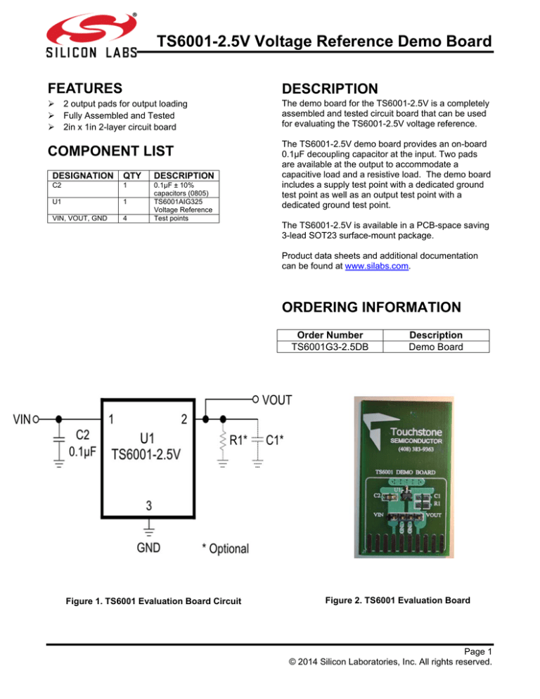
The demo board for the TS6001-2.5V is a completely
assembled and tested circuit board that can be used
for evaluating the TS6001-2.5V voltage reference.
2 output pads for output loading
Fully Assembled and Tested
2in x 1in 2-layer circuit board
COMPONENT LIST
DESIGNATION
QTY
DESCRIPTION
C2
1
U1
1
VIN, VOUT, GND
4
0.1µF ± 10%
capacitors (0805)
TS6001AIG325
Voltage Reference
Test points
The TS6001-2.5V demo board provides an on-board
0.1µF decoupling capacitor at the input. Two pads
are available at the output to accommodate a
capacitive load and a resistive load. The demo board
includes a supply test point with a dedicated ground
test point as well as an output test point with a
dedicated ground test point.
The TS6001-2.5V is available in a PCB-space saving
3-lead SOT23 surface-mount package.
Product data sheets and additional documentation
can be found at www.silabs.com.
ORDERING INFORMATION
Order Number
TS6001G3-2.5DB
Figure 1. TS6001 Evaluation Board Circuit
Description
Demo Board
Figure 2. TS6001 Evaluation Board
Page 1
© 2014 Silicon Laboratories, Inc. All rights reserved.
TS6001 Voltage Reference Demo Board
DESCRIPTION
The demo board provides an on-board 0.1µF
decoupling capacitor at the VIN input. Two pads are
available at the output to accommodate a capacitive
load and a resistive load as needed.
QUICK START PROCEDURES
Required Equipment
TS6001DB demo board
A DC Power Supply, Single, an HP Model
HP6624A or equivalent
A digital voltmeter, an HP34410A or equivalent
A digital ammeter, an HP34410A or equivalent
To evaluate the TS6001 voltage reference, the
following steps are to be performed:
1) Before connecting the DC power supply to the
demo board, turn on the power supply and set
the DC voltage to 5V and then turn it off.
2) Connect the DC power supply positive terminal to
the negative terminal of the digital ammeter.
Then, connect the positive terminal of the
ammeter to the test point VIN and the negative
terminal of the DC power supply to the adjacent
test point GND.
6) The input voltage VIN can vary from VOUT +
0.2V to 12.6V as needed. Please refer to the
TS6001 product datasheet “Electrical
Characteristics” section for more information.
Note: In order to add a Kelvin connection to the
output test point VOUT, connect the positive terminal
of a DVM to VOUT and the negative terminal to GND.
Then, place a resistor and/or capacitor on pads R1
and/or pads C1, respectively. For an accurate VOUT
measurement, always connect the positive terminal of
the DVM to the VOUT test point.
If additional loading is needed on the output VOUT, a
wire can be soldered on pads R1 and C1. Then, a
load can be connected to the other end of the wire.
Make sure the load is connected to the ground on the
board.
Figure 4. Top Layer Trace
View
Page 2 Silicon Laboratories, Inc.
400 West Cesar Chavez, Austin, TX 78701
+1 (512) 416-8500 ▪ www.silabs.com
4) An optional load resistor ≥ 5kΩ and capacitor up
to 2200pF can be soldered on the board. Solder
the resistor on pads R1 and the capacitor on
pads C1. If a load is not desired, leave these
pads open and proceed to step 5.
5) Turn on the power supply and check that the
digital voltmeter is reading an output voltage
within ±0.2% of 2.5V and the digital ammeter is
reading a supply current less than 35µA.
Figure 3. Top Layer Component
View
3) Connect the positive terminal of the digital
voltmeter to test point VOUT and the negative
terminal to the adjacent test point GND.
Figure 5. Bottom layer (GND)
TS6001-EVB Rev. 1.0
Smart.
Connected.
Energy-Friendly
Products
Quality
Support and Community
www.silabs.com/products
www.silabs.com/quality
community.silabs.com
Disclaimer
Silicon Laboratories intends to provide customers with the latest, accurate, and in-depth documentation of all peripherals and modules available for system and software implementers
using or intending to use the Silicon Laboratories products. Characterization data, available modules and peripherals, memory sizes and memory addresses refer to each specific
device, and "Typical" parameters provided can and do vary in different applications. Application examples described herein are for illustrative purposes only. Silicon Laboratories
reserves the right to make changes without further notice and limitation to product information, specifications, and descriptions herein, and does not give warranties as to the accuracy
or completeness of the included information. Silicon Laboratories shall have no liability for the consequences of use of the information supplied herein. This document does not imply
or express copyright licenses granted hereunder to design or fabricate any integrated circuits. The products must not be used within any Life Support System without the specific
written consent of Silicon Laboratories. A "Life Support System" is any product or system intended to support or sustain life and/or health, which, if it fails, can be reasonably expected
to result in significant personal injury or death. Silicon Laboratories products are generally not intended for military applications. Silicon Laboratories products shall under no
circumstances be used in weapons of mass destruction including (but not limited to) nuclear, biological or chemical weapons, or missiles capable of delivering such weapons.
Trademark Information
Silicon Laboratories Inc., Silicon Laboratories, Silicon Labs, SiLabs and the Silicon Labs logo, CMEMS®, EFM, EFM32, EFR, Energy Micro, Energy Micro logo and combinations
thereof, "the world’s most energy friendly microcontrollers", Ember®, EZLink®, EZMac®, EZRadio®, EZRadioPRO®, DSPLL®, ISOmodem ®, Precision32®, ProSLIC®, SiPHY®,
USBXpress® and others are trademarks or registered trademarks of Silicon Laboratories Inc. ARM, CORTEX, Cortex-M3 and THUMB are trademarks or registered trademarks of
ARM Holdings. Keil is a registered trademark of ARM Limited. All other products or brand names mentioned herein are trademarks of their respective holders.
Silicon Laboratories Inc.
400 West Cesar Chavez
Austin, TX 78701
USA
http://www.silabs.com


