10 V Precision
Voltage Reference
REF01
FEATURES
PIN CONFIGURATIONS
10 V output, ±0.3% maximum
Adjustment range, ±3% minimum
Excellent temperature stability, 8.5 ppm/°C maximum
Low noise, 30 µV p-p maximum
Low supply current, 1.4 mA maximum
Wide input voltage range, 12 V to 40 V
High load driving capability, 10 mA
No external components
Short-circuit proof
NC
8
NC 1
7
VIN 2
NC
6
NC 3
5
VOUT
TRIM
4
NC = NO CONNECT. DO NOT CONNECT ANYTHING
ON THESE PINS. SOME OF THEM ARE RESERVED
FOR FACTORY TESTING PURPOSES.
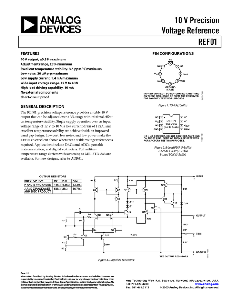
Figure 1. TO-99 (J Suffix)
GENERAL DESCRIPTION
The REF01 precision voltage reference provides a stable 10 V
output that can be adjusted over a 3% range with minimal effect
on temperature stability. Single-supply operation over an input
voltage range of 12 V to 40 V, a low current drain of 1 mA, and
excellent temperature stability are achieved with an improved
band gap design. Low cost, low noise, and low power make the
REF01 an excellent choice whenever a stable voltage reference is
required. Applications include DACs and ADCs, portable
instrumentation, and digital voltmeters. Full military
temperature range devices with screening to MIL-STD-883 are
available. For new designs, refer to ADR01.
NC 1
8
REF01
NC
NC
TOP VIEW
6 VOUT
(Not to Scale)
5 TRIM
GND 4
VIN 2
7
NC = NO CONNECT. DO NOT CONNECT ANYTHING
ON THESE PINS. SOME OF THEM ARE RESERVED
FOR FACTORY TESTING PURPOSES.
00373-F-002
NC 3
Figure 2. 8-Lead PDIP (P-Suffix)
8-Lead CERDIP (Z-Suffix)
8-Lead SOIC (S-Suffix)
INPUT
OUTPUT RESISTORS
R11
00373-F-001
GROUND
(CASE)
R7
R8
REF01 OPTION
R9
R12
P AND S PACKAGES
18kΩ 4.5kΩ
33.3kΩ
J AND Z PACKAGES,
AND 883C PRODUCT
50kΩ 2kΩ
16.7kΩ
2
R14
Q15
Q7
Q8
Q14
R15
Q13
Q18
Q9
Q12
Q16
Q11
C1
Q10
R6
R3
Q6
Q19
Q21
Q17
Q5
OUTPUT
6
R13
R4
R12*
Q4
Q1
R1
Q2
Q3
Q20
R9*
TRIM
≈1.23V
5
R11*
R10
R2
GROUND
*SEE OUTPUT RESISTORS
4
00373-F-003
R5
Figure 3. Simplified Schematic
Rev. H
Information furnished by Analog Devices is believed to be accurate and reliable. However, no
responsibility is assumed by Analog Devices for its use, nor for any infringements of patents or other
rights of third parties that may result from its use. Specifications subject to change without notice. No
license is granted by implication or otherwise under any patent or patent rights of Analog Devices.
Trademarks and registered trademarks are the property of their respective owners.
One Technology Way, P.O. Box 9106, Norwood, MA 02062-9106, U.S.A.
Tel: 781.329.4700
www.analog.com
Fax: 781.461.3113
© 2005 Analog Devices, Inc. All rights reserved.
REF01
TABLE OF CONTENTS
Features .............................................................................................. 1
ESD Caution...................................................................................5
General Description ......................................................................... 1
Typical Performance Characteristics ..............................................6
Pin Configurations ........................................................................... 1
Applications........................................................................................8
Revision History ............................................................................... 2
Precision Current Source .......................................................... 10
Specifications..................................................................................... 3
Supply Bypassing ........................................................................ 10
Electrical Specifications............................................................... 3
Reference Stack with Excellent Line Regulation .................... 10
Absolute Maximum Ratings............................................................ 5
Outline Dimensions ....................................................................... 11
Thermal Resistance ...................................................................... 5
Ordering Guide .......................................................................... 12
REVISION HISTORY
12/05—Rev. G to Rev. H
Changes to Figure 12........................................................................ 8
Changes to Ordering Guide .......................................................... 12
2/05—Rev. F to Rev. G
Changes to Electrical Specifications .............................................. 3
Changes to Electrical Specifications .............................................. 4
7/04—Rev. E to Rev. F
Updated Format..................................................................Universal
Changes to Simplified Schematic ................................................... 1
Changes to Specifications ................................................................ 3
Changes to Specifications ................................................................ 4
Changes to Applications .................................................................. 8
Changes to Ordering Guide ............................................................ 9
2/04—Rev. D to Rev. E
Changes to Simplified Schematic .................................................. 1
Changes to Ordering Guide ............................................................ 4
Replaced Figure 6 ............................................................................. 5
Replaced Figure 7 ............................................................................. 5
10/03—Rev. C to Rev. D
Changes to Features ..........................................................................1
Changes to Electrical Specifications ...............................................2
Deleted Figure 13...............................................................................3
Deleted Wafer Test Limits ................................................................4
Deleted Typical Electrical Characteristics......................................4
Changes to Ordering Guide .............................................................4
Updated Outline Dimensions..........................................................8
10/02—Rev. B to Rev. C
Edits to Features.................................................................................1
Delete RC-Suffix................................................................................1
Edits to Absolute Maximum Ratings ..............................................5
Edits to Ordering Guide ...................................................................5
Edits to Package Type .......................................................................5
Delete CP-20 ......................................................................................9
Updated Outline Dimensions..........................................................9
Rev. H | Page 2 of 12
REF01
SPECIFICATIONS
ELECTRICAL SPECIFICATIONS
@ VIN = 15 V, TA = 25°C, unless otherwise noted.
Table 1.
Parameter
Output Voltage
Output Adjustment Range
Output Voltage Noise1
S, Z, P Packages
J, 883 Parts
Line Regulation2
Load Regulation2
Turn-On Settling Time3
Quiescent Supply Current
Load Current
Sink Current4
Short-Circuit Current
REF01A/REF01E
Min
Typ
Max
9.97
10.00
10.03
±3.0
±3.3
Symbol
VO
∆VTRIM
Conditions
IL = 0 mA
RP = 10 kΩ
en p-p
en p-p
0.1 Hz to 10 Hz
0.1 Hz to 10 Hz
VIN = 13 V to 33 V
IL = 0 mA to 10 mA
To ± 0.1% of final value
No load
tON
ISY
IL
IS
ISC
30
35
0.006
0.005
5
1.0
10
−0.3
REF01H
Typ
Max
10.00
10.05
±3.3
30
35
0.006
0.006
5
1.0
0.010
0.008
1.4
10
−0.3
−0.5
30
VO = 0
Min
9.95
±3.0
0.010
0.010
1.4
−0.5
30
Unit
V
%
µV p-p
µV p-p
%/V
%/mA
µs
mA
mA
mA
mA
1
Sample tested.
Line and load regulation specifications include the effect of self-heating.
3
Guaranteed by design, not production tested.
4
During sink current test, the device meets the output voltage specified.
2
@ VIN = 15 V, −55°C ≤ TA ≤ +125°C for REF01A/REF01E, and 0°C ≤ TA ≤ 70°C for REF01H, and IL = 0 mA, unless otherwise noted.
Table 2.
Parameter
Output Voltage Change
with Temperature1, 2
Output Voltage
Temperature Coefficient3
Change in VO Temperature Coefficient
with Output Adjustment
Line Regulation
(VIN = 13 V to 33 V)4
Load Regulation
(IL = 0 mA to 8 mA)4
1
3
TCVO
RP = 10 kΩ
0.7
0°C ≤ TA ≤ 70°C
−55°C ≤ TA ≤ + 125°C
0°C ≤ TA ≤ 70°C
−55°C ≤ TA ≤ + 125°C
0.007
0.009
0.006
0.007
VMAX − VMIN
× 100
10 V
∆VOT specification applies trimmed to 10000 V or untrimmed.
TCVO is defined as ∆Var divided by the temperature range; therefore,
∆VOT (0°C to + 70°C) and
TCVO (0°C to + 70°C) =
4
Conditions
0°C ≤ TA ≤ 70°C
−55°C ≤ TA ≤+ 125°C
Min
REF01H
Typ
0.07
0.18
10.0
Max
0.17
0.45
25.0
0.7
0.012
0.015
0.010
0.012
0.007
0.009
0.007
0.009
Unit
%
%
ppm/°C
ppm/%
0.012
0.015
0.012
0.015
%/V
%/V
%/mA
%/mA
∆VOT is defined as the absolute difference between the maximum output voltage and the minimum output voltage over the specified temperature range expressed as
a percentage of 10 V:
∆VOT =
2
Symbol
∆VOT
REF01A/REF01E
Min Typ
Max
0.02
0.06
0.06
0.15
3.0
8.5
70°C
TCVO (− 55°C to + 125°C) =
∆VOT (− 55°C to + 125°C)
180°C
Line and load regulation specifications include the effect of self-heating.
Rev. H | Page 3 of 12
REF01
@ VIN = 15 V, TA = 25°C, unless otherwise noted.
Table 3.
Parameter
Output Voltage
Output Adjustment Range
Output Voltage Noise1
S, Z, P Packages
J, 883 Parts
Line Regulation2
Load Regulation2
Turn-On Settling Time3
Quiescent Supply Current
Load Current
Sink Current4
Short-Circuit Current
Symbol
VO
∆VTRIM
Conditions
IL = 0 mA
RP = 10 kΩ
e n p-p
e n p-p
0.1 Hz to 10 Hz
0.1 Hz to 10 Hz
VIN = 13 V to 33 V
IL = 0 mA to 8 mA
To ±0.1% of final value
No load
tON
ISY
IL
IS
ISC
REF01C
Typ
10.00
±3.3
Min
9.90
±2.7
Max
10.10
30
35
µV p-p
µV p-p
0.009
0.006
5
1.0
8
−0.3
0.015
0.015
1.6
−0.5
30
VO = 0
Unit
V
%
%/V
%/mA
µs
mA
mA
mA
mA
1
Sample tested.
Line and load regulation specifications include the effect of self-heating.
Guaranteed by design, not production tested.
4
During sink current test, the device meets the output voltage specified.
2
3
@ VIN = 15 V, 0°C ≤ TA ≤ +70°C for REF01CJ, REF01CZ, and −40°C ≤ TA ≤ +85°C for REF01CP and REF01CS, unless otherwise noted.
Table 4.
Parameter
Output Voltage Change
with Temperature1, 2
Output Voltage
Temperature Coefficient3
Change in VO Temperature
Coefficient with Output
Adjustment
Line Regulation4
Load Regulation4
1
3
TCVO
RP = 10 kΩ
VIN =13 V to 30 V
IL = 0 to 5 mV
V MAX − V MIN
×100
10 V
∆VOT specification applies trimmed to +10,000 V or untrimmed.
TCVO is defined as ∆Var divided by the temperature range; therefore,
∆VOT (0°C to + 70°C) and
TCVO (0°C to + 70°C) =
4
Conditions
Min
REF01C
Typ
0.14
Max
0.45
Unit
%
20
65
ppm/°C
0.018
0.018
ppm/°C
%/V
%/mA
0.7
0.011
0.008
∆VOT is defined as the absolute difference between the maximum output voltage and the minimum output voltage over the specified temperature range expressed as
a percentage of 10 V:
∆VOT =
2
Symbol
∆VOT
70°C
TCVO (− 55°C to + 125°C) =
∆VOT (− 55°C to + 125°C)
180°C
Line and load regulation specifications include the effect of self-heating.
Rev. H | Page 4 of 12
REF01
ABSOLUTE MAXIMUM RATINGS
Table 5.
Parameter
Input Voltage
Output Short-Circuit Duration
(to Ground or VIN)
Storage Temperature Range
J, S, and Z Packages
P Package
Operating Temperature Range
REF01A
REF01CJ
REF01CP, REF01CS, REF01E, REF01H
Junction Temperature (TJ)
Lead Temperature (Soldering @ 60 sec)
1
THERMAL RESISTANCE
Rating1
40 V
Table 6.
Indefinite
−65°C to +150°C
−65°C to +125°C
Package Type
TO-99 (J)
8-Lead CERDIP (Z)
8-Lead PDIP (P)
8-Pin SOIC (S)
1
−55°C to +125°C
0°C to 70°C
−40°C to +85°C
−65°C to +150°C
300°C
θJA1
170
162
110
160
θJC
24
26
50
44
Unit
°C/W
°C/W
°C/W
°C/W
θJA is specified for worst-case mounting conditions; that is, θJA is specified for
device in socket for TO, CERDIP, and PDIP packages. θJA is specified for device
soldered to printed circuit board for SOIC package.
Absolute maximum ratings apply to both DICE and packaged parts, unless
otherwise noted.
Stresses above those listed under Absolute Maximum Ratings
may cause permanent damage to the device. This is a stress
rating only; functional operation of the device at these or any
other conditions above those indicated in the operational
section of this specification is not implied. Exposure to absolute
maximum rating conditions for extended periods may affect
device reliability.
ESD CAUTION
ESD (electrostatic discharge) sensitive device. Electrostatic charges as high as 4000 V readily accumulate on
the human body and test equipment and can discharge without detection. Although this product features
proprietary ESD protection circuitry, permanent damage may occur on devices subjected to high energy
electrostatic discharges. Therefore, proper ESD precautions are recommended to avoid performance
degradation or loss of functionality.
Rev. H | Page 5 of 12
REF01
TYPICAL PERFORMANCE CHARACTERISTICS
76
0.0031
66
0.0100
56
0.0310
46
0.1000
36
0.3100
26
1.0000
20
100
1k
10k
FREQUENCY (Hz)
10.0000
1M
100k
MAXIMUM LOAD CURRENT (mA)
LINE REGULATION (%/V)
19
18
17
16
15
14
10
Figure 4. Line Regulation vs. Frequency
15
20
25
30
INPUT VOLTAGE (V)
35
40
Figure 7. Maximum Load Current vs. Input Voltage
1.4
VIN = 15V
TA = 25°C
VIN = 15V
LOAD REG–T/LOAD REG (25°C)
1.3
1k
00373-F-007
100
10
10
100
1k
10k
FREQUENCY (Hz)
100k
1.1
1.0
0.9
0.8
0.7
0.6
–60
1M
Figure 5. Output Wideband Noise vs. Bandwidth
(0.1 Hz to Frequency Indicated)
1.2
00373-F-010
10k
–40
–20
0
20
40
60
80
TEMPERATURE (°C)
100
120
140
Figure 8. Normalized Load Regulation (∆IL = 10 mA) vs. Temperature
1.4
0.016
VIN = 15V
1.3
LINE REG–T/LINE REG (25°C)
0.014
0.012
0.010
0.008
0.006
0.004
0
–10
25°C
0
10
20
TIME (s)
00373-F-008
0.002
DEVICE IMMERSED
IN 75°C OIL BATH
30
40
50
1.2
1.1
1.0
0.9
0.8
00373-F-011
OUTPUT NOISE (µV p-p)
00373-F-009
0
10
3.1000
00373-F-006
VIN = 15V
TA = 25°C
16
PERCENT CHANGE IN OUTPUT VOLTAGE (%)
LINE REGULATION (dB)
TA = 25°C
0.7
0.6
–60
–40
–20
0
20
40
60
80
TEMPERATURE (°C)
100
120
Figure 9. Normalized Line Regulation vs. Temperature
Figure 6. Output Change due to Thermal Shock
Rev. H | Page 6 of 12
140
REF01
30
1.3
VIN = 15V
1.2
20
15
10
5
0
–60
–40
–20
0
20
40
60
80
TEMPERATURE (°C)
100
120
140
Figure 10. Maximum Load Current vs. Temperature
1.1
1.0
0.9
0.8
0.7
–60
00373-F-013
QUIESCENT CURRENT (mA)
25
00373-F-012
MAXIMUM LOAD CURRENT (mA)
VIN = 15V
–40
–20
0
20
40
60
80
TEMPERATURE (°C)
100
Figure 11. Quiescent Current vs. Temperature
Rev. H | Page 7 of 12
120
140
REF01
APPLICATIONS
1.1mA
U1
REF01
2
VO
TEMP TRIM
GND
9V
pot
10kΩ
R1
470kΩ
VO
+
6
0.1µF
REF01
9V
TRIM
GND
00373-022
R2
1kΩ
5
100kΩ
4
–
Figure 15. Precision Calibration Standard
Figure 12. Output Adjustment
The REF01 trim terminal can be used to adjust the output
voltage over a 10 V ± 300 mV range. This feature lets the
system designer trim system errors by setting the reference
to a voltage other than 10 V. The output also can be set exactly
to 10.000 V or to 10.240 V for binary applications.
15V
VOLTAGE COMPLIANCE: –25V TO +3V
2
VIN
VO
6
REF01
Adjustment of the output does not significantly affect the
temperature performance of the device. The temperature
coefficient change is approximately 0.7 ppm/°C for 100 mV
of output adjustment.
TRIM
5
R
IOUT = 10V + 1mA
R
GND
4
+18V
IOUT
VIN
Figure 16. Current Source
+15V
ANALOG
INPUT
0V TO +10V +15V
–15V +15V
2
VIN
VO
0.01µF
6
00373-F-005
GND
–18V
0.1µF
GND TRIM
Figure 13. Burn-In Circuit
5kΩ
LSB
B1 B2 B3 B4 B5 B6 B7 B8
lO
4
lO
2
DAC08
REF01
V+
GND
4
V–
OP02
EO
5kΩ
+15V
SERIAL
OUTPUT
START
VLC
CC
14
13
IO
DAC08
3
2
IO
8
4
2
6
7 8 9 10 11 12 1
B1 B2 B3 B4 B5 B6 B7 B8
E
POS. FULL SCALE –1LSB
1
1
1
1
1
1
1
1
+4.960
ZERO SCALE
1
0
0
0
0
0
0
0
0.000
NEG. FULL SCALE +1LSB
0
0
0
0
0
0
0
1
–4.960
NEG. FULL SCALE
0
0
0
0
0
0
0
0
–5.000
1kΩ
1
10
7
AM2592
SUCCESSIVEAPPROXIMATION
REGISTER
Figure 17. DAC Reference
Figure 14. Burn-In Circuit
Rev. H | Page 8 of 12
CONNECT START TO
CONVERSION COMPLETE
FOR CONTINUOUS
CONVERSION
9
CONVERSION TTL CLOCK
COMPLETE INPUT 2.25MHz
–15V
4
–15V
2
–15V
7
CMP01C
1
5
14 13 12 11 6 5 4 3
00373-F-014
0.1µF
5kΩ
3.9MΩ
3
16
15
+15V
5kΩ
5
B1
B2
B3
B4
B5
B6
B7
B8
10kΩ
MSB
5kΩ
5kΩ
4
+15V
CC
REF01
00373-F-017
REF01
2
6
VIN V
O
5
10V
00373-F-015
VOUT
VIN
VIN
00373-F-016
VIN
REF01
+15V
2
IOUT
+10V
VO 6
VOLTAGE COMPLIANCE: –3V TO +25V
2
VIN
REF01
10kΩ ± 0.1%
TRIM
GND
5
VO
10kΩ ± 0.1%
REF01
+15V
4
0.1µF
TRIM
–10V
OP02
–15V
5
R
IOUT = 10V + 1mA
R
GND
4
00373-F-018
5kΩ
6
00373-F-019
VIN
–15V
Figure 18. ±10 V Reference
Figure 19. Current Sink
Rev. H | Page 9 of 12
REF01
PRECISION CURRENT SOURCE
SUPPLY BYPASSING
A current source with 25 V output compliance and excellent
output impedance can be obtained using this circuit. REF01
keeps the line voltage and power dissipation constant in the
device; the only important error consideration at room
temperature is the negative supply rejection of the op amp.
The typical 3 µV/V PSRR of the OP02E creates an 8 ppm
change (3 µV/V × 25 V/10 V) in output current over a 25 V
range. For example, a 10 mA current source can be built
(R = 1 kΩ) with 300 MΩ output impedance.
For best results, it is recommended that the power supply pin be
bypassed with a 0.1 µF disc ceramic capacitor.
RO =
REFERENCE STACK WITH EXCELLENT LINE
REGULATION
Three REF01s can be stacked to yield 10 V, 20 V, and 30 V
outputs. An additional advantage is near-perfect line regulation
of the 10.0 V and 20.0 V output. A 32 V to 60 V input change
produces an output change that is less than the noise voltage of
the devices. A load bypass resistor (RB) provides a path for the
supply current (ISY) of the 20 V regulator.
25 V
8 × 10 −6 × 10 mA
In general, any number of REF01s can be stacked this way.
For example, 10 devices will yield outputs of 10 V, 20 V,
30 V . . . 100 V. The line voltage can change from 105 V to
130 V. However, care must be taken to ensure that the total
load currents do not exceed the maximum usable current
(typically 21 mA).
+50V
6
2
VIN
32V TO 60V
VO
TRIMMED
OUTPUTS
2
VIN
REF01
30V
6
VO
2
REF01
GND
4
2
VO
TRIM
5
10kΩ
GND
6
4
REF01
C
1
2
R
(TRIM FOR
CALIBRATION)
VIN
GND
VO
6
20V
REF01
4
R
TRIM
GND
2
C
VIN
7
6
OP02E
6
5
4
10kΩ
10V
VO
2
3
VO = 0V
TO 25V
REF01
TRIM
4
5
10kΩ
RB
6.8kΩ
GND
–5V
10V
IO =
R
00373-F-020
RC = 10–5 SEC
Figure 20. Precision Current Source
00373-F-021
VIN
4
Figure 21. Reference Stack
Rev. H | Page 10 of 12
REF01
OUTLINE DIMENSIONS
0.005 (0.13)
MIN
8
0.055 (1.40)
MAX
5
5.00 (0.1968)
4.80 (0.1890)
0.310 (7.87)
0.220 (5.59)
1
4
8
1.27 (0.0500)
BSC
0.060 (1.52)
0.015 (0.38)
0.200 (5.08)
MAX
0.25 (0.0098)
0.10 (0.0040)
0.150 (3.81)
MIN
0.200 (5.08)
0.125 (3.18)
0.070 (1.78)
0.030 (0.76)
6.20 (0.2440)
4 5.80 (0.2284)
0.320 (8.13)
0.290 (7.37)
0.405 (10.29) MAX
0.023 (0.58)
0.014 (0.36)
5
4.00 (0.1574)
3.80 (0.1497) 1
0.100 (2.54) BSC
SEATING
PLANE
0.51 (0.0201)
COPLANARITY
SEATING 0.31 (0.0122)
0.10
PLANE
0.015 (0.38)
0.008 (0.20)
15°
0°
1.75 (0.0688)
1.35 (0.0532)
0.50 (0.0196)
× 45°
0.25 (0.0099)
8°
0.25 (0.0098) 0° 1.27 (0.0500)
0.40 (0.0157)
0.17 (0.0067)
COMPLIANT TO JEDEC STANDARDS MS-012-AA
CONTROLLING DIMENSIONS ARE IN MILLIMETERS; INCH DIMENSIONS
(IN PARENTHESES) ARE ROUNDED-OFF MILLIMETER EQUIVALENTS FOR
REFERENCE ONLY AND ARE NOT APPROPRIATE FOR USE IN DESIGN.
CONTROLLING DIMENSIONS ARE IN INCHES; MILLIMETER DIMENSIONS
(IN PARENTHESES) ARE ROUNDED-OFF INCH EQUIVALENTS FOR
REFERENCE ONLY AND ARE NOT APPROPRIATE FOR USE IN DESIGN.
Figure 24. 8-Lead Standard Small Outline Package [SOIC]
Narrow Body
(R-8)
S-Suffix
Dimensions shown in millimeters and (inches
Figure 22. 8-Lead Ceramic Dual In-Line Package [CERDIP]
(Q-8)
Z-Suffix
Dimensions shown in inches and (millimeters)
0.400 (10.16)
0.365 (9.27)
0.355 (9.02)
8
5
REFERENCE PLANE
1
0.1850 (4.70)
0.1650 (4.19)
0.5000 (12.70)
MIN
0.2500 (6.35) MIN
0.0500 (1.27) MAX
0.1600 (4.06)
0.1400 (3.56)
0.3350 (8.51)
0.3050 (7.75)
0.3700 (9.40)
0.3350 (8.51)
5
6
4
3
7
2
0.0400 (1.02) MAX
0.0400 (1.02)
0.0100 (0.25)
0.0190 (0.48)
0.0160 (0.41)
0.1000
(2.54)
BSC
0.0210 (0.53)
0.0160 (0.41)
0.325 (8.26)
0.310 (7.87)
0.300 (7.62)
PIN 1
0.1000 (2.54)
BSC
0.2000
(5.08)
BSC
4
0.280 (7.11)
0.250 (6.35)
0.240 (6.10)
8
0.0450 (1.14)
0.0270 (0.69)
0.100 (2.54)
BSC
0.210
(5.33)
MAX
0.150 (3.81)
0.130 (3.30)
0.115 (2.92)
1
0.0340 (0.86)
0.0280 (0.71)
0.060 (1.52)
MAX
0.015
(0.38)
MIN
0.195 (4.95)
0.130 (3.30)
0.115 (2.92)
0.015 (0.38)
GAUGE
PLANE
0.014 (0.36)
0.010 (0.25)
0.008 (0.20)
SEATING
PLANE
0.022 (0.56)
0.018 (0.46)
0.014 (0.36)
0.005 (0.13)
MIN
0.430 (10.92)
MAX
0.070 (1.78)
0.060 (1.52)
0.045 (1.14)
45° BSC
BASE & SEATING PLANE
COMPLIANT TO JEDEC STANDARDS MO-002-AK
CONTROLLING DIMENSIONS ARE IN INCHES; MILLIMETER DIMENSIONS
(IN PARENTHESES) ARE ROUNDED-OFF INCH EQUIVALENTS FOR
REFERENCE ONLY AND ARE NOT APPROPRIATE FOR USE IN DESIGN.
Figure 23. 8-Lead Metal Header [TO-99]
(H-08)
J-Suffix
Dimensions shown in inches and (millimeters)
COMPLIANT TO JEDEC STANDARDS MS-001-BA
CONTROLLING DIMENSIONS ARE IN INCHES; MILLIMETER DIMENSIONS
(IN PARENTHESES) ARE ROUNDED-OFF INCH EQUIVALENTS FOR
REFERENCE ONLY AND ARE NOT APPROPRIATE FOR USE IN DESIGN.
CORNER LEADS MAY BE CONFIGURED AS WHOLE OR HALF LEADS.
Figure 25. 8-Lead Plastic Dual In-Line Package [PDIP]
Narrow Body
(N-8)
P-Suffix
Dimensions shown in inches and (millimeters)
Rev. H | Page 11 of 12
REF01
ORDERING GUIDE
Model
REF01AJ/883C
REF01EJ
REF01CJ
REF01EZ
REF01HZ
REF01AZ/883C
REF01CP
REF01CPZ2
REF01HPZ2
REF01HP
REF01HS3
REF01HS-REEL3
REF01HSZ2, 3
REF01HSZ-REEL2, 3
REF01CS3
REF01CS-REEL3
REF01CS-REEL73
REF01CSZ-REEL2, 3
REF01CSZ-REEL72, 3
REF01CSZ2, 3
1
2
3
TA = 25° C
∆VOS Max (mV)
±30
±30
±100
±30
±50
±30
±100
±100
±50
±50
±50
±50
±50
±50
±100
±100
±100
±100
±100
±100
Temperature Range (°C)
−55 to +125
−40 to +85
0 to 70
−40 to +85
−40 to +85
−55 to +125
−40 to +85
−40 to +85
−40 to +85
−40 to +85
−40 to +85
−40 to +85
−40 to +85
−40 to +85
−40 to +85
−40 to +85
−40 to +85
−40 to +85
−40 to +85
−40 to +85
Package Description1
8-Lead TO-99
8-Lead TO-99
8-Lead TO-99
8-Lead CERDIP
8-Lead CERDIP
8-Lead CERDIP
8-Lead PDIP
8-Lead PDIP
8-Lead PDIP
8-Lead PDIP
8-Lead SOIC
8-Lead SOIC
8-Lead SOIC
8-Lead SOIC
8-Lead SOIC
8-Lead SOIC
8-Lead SOIC
8-Lead SOIC
8-Lead SOIC
8-Lead SOIC
Burn-in is available on commercial and industrial temperature range parts in CERDIP, PDIP, and TO-99 packages.
Z = Pb-free part.
For availability and burn-in information on SOIC packages, contact your local Sales office.
© 2005 Analog Devices, Inc. All rights reserved. Trademarks and
registered trademarks are the property of their respective owners.
C00373-0-12/05(H)
Rev. H | Page 12 of 12
Package Option
J-Suffix (H-08)
J-Suffix (H-08)
J-Suffix (H-08)
Z-Suffix (Q-8)
Z-Suffix (Q-8)
Z-Suffix (Q-8)
P-Suffix (N-8)
P-Suffix (N-8)
P-Suffix (N-8)
P-Suffix (N-8)
S-Suffix (R-8)
S-Suffix (R-8)
S-Suffix (R-8)
S-Suffix (R-8)
S-Suffix (R-8)
S-Suffix (R-8)
S-Suffix (R-8)
S-Suffix (R-8)
S-Suffix (R-8)
S-Suffix (R-8)
