High Speed, High Voltage,
1 A Output Drive Amplifier
ADA4870-KGD
Known Good Die
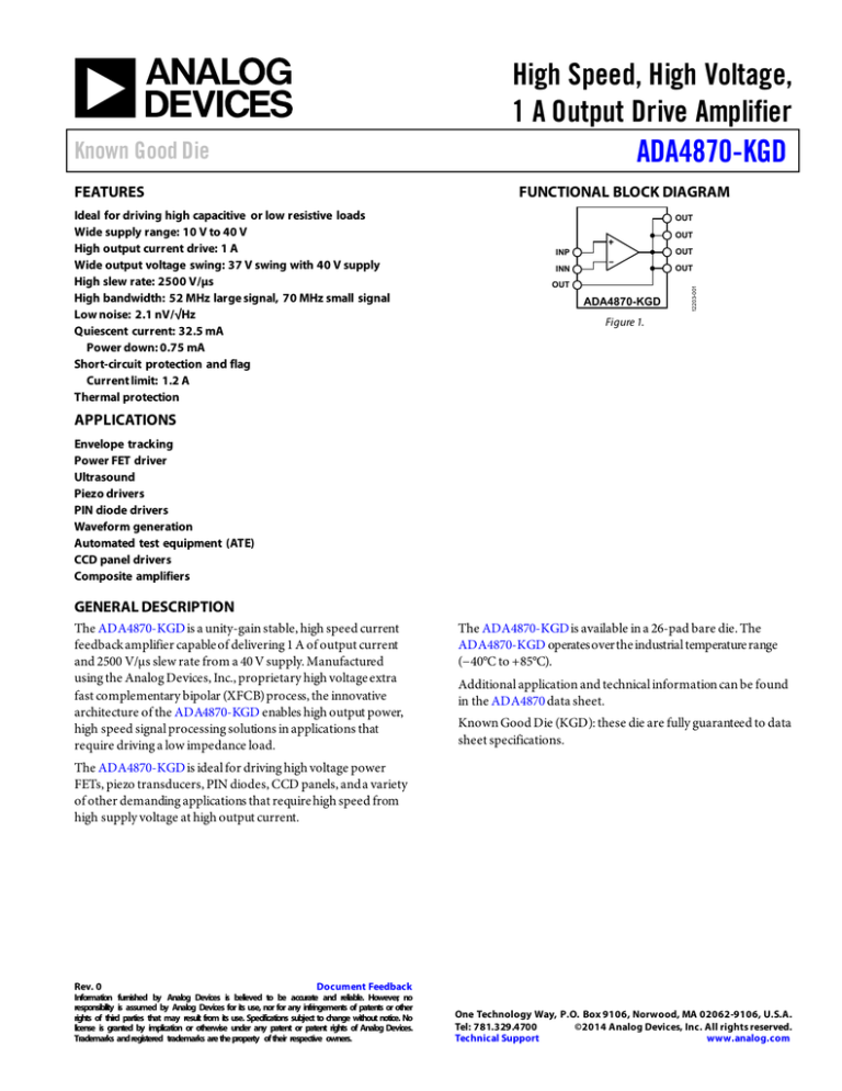
FUNCTIONAL BLOCK DIAGRAM
Ideal for driving high capacitive or low resistive loads
Wide supply range: 10 V to 40 V
High output current drive: 1 A
Wide output voltage swing: 37 V swing with 40 V supply
High slew rate: 2500 V/µs
High bandwidth: 52 MHz large signal, 70 MHz small signal
Low noise: 2.1 nV/√Hz
Quiescent current: 32.5 mA
Power down: 0.75 mA
Short-circuit protection and flag
Current limit: 1.2 A
Thermal protection
OUT
OUT
INP
OUT
INN
OUT
OUT
ADA4870-KGD
12203-001
FEATURES
Figure 1.
APPLICATIONS
Envelope tracking
Power FET driver
Ultrasound
Piezo drivers
PIN diode drivers
Waveform generation
Automated test equipment (ATE)
CCD panel drivers
Composite amplifiers
GENERAL DESCRIPTION
The ADA4870-KGD is a unity-gain stable, high speed current
feedback amplifier capable of delivering 1 A of output current
and 2500 V/µs slew rate from a 40 V supply. Manufactured
using the Analog Devices, Inc., proprietary high voltage extra
fast complementary bipolar (XFCB) process, the innovative
architecture of the ADA4870-KGD enables high output power,
high speed signal processing solutions in applications that
require driving a low impedance load.
The ADA4870-KGD is available in a 26-pad bare die. The
ADA4870-KGD operates over the industrial temperature range
(−40°C to +85°C).
Additional application and technical information can be found
in the ADA4870 data sheet.
Known Good Die (KGD): these die are fully guaranteed to data
sheet specifications.
The ADA4870-KGD is ideal for driving high voltage power
FETs, piezo transducers, PIN diodes, CCD panels, and a variety
of other demanding applications that require high speed from
high supply voltage at high output current.
Rev. 0
Document Feedback
Information furnished by Analog Devices is believed to be accurate and reliable. However, no
responsibility is assumed by Analog Devices for its use, nor for any infringements of patents or other
rights of third parties that may result from its use. Specifications subject to change without notice. No
license is granted by implication or otherwise under any patent or patent rights of Analog Devices.
Trademarks and registered trademarks are the property of their respective owners.
One Technology Way, P.O. Box 9106, Norwood, MA 02062-9106, U.S.A.
Tel: 781.329.4700
©2014 Analog Devices, Inc. All rights reserved.
Technical Support
www.analog.com
ADA4870-KGD
Known Good Die
TABLE OF CONTENTS
Features........................................................................................... 1
Absolute Maximum Ratings ......................................................... 6
Applications ................................................................................... 1
ESD Caution............................................................................... 6
Functional Block Diagram............................................................ 1
Pin Configuration and Function Descriptions............................ 7
General Description ...................................................................... 1
Outline Dimensions ...................................................................... 8
Revision History ............................................................................ 2
Die Specifications and Assembly Recommendations ............. 8
Specifications ................................................................................. 3
Ordering Guide.......................................................................... 8
±20 V Supply.............................................................................. 3
±5 V Supply................................................................................ 4
REVISION HISTORY
10/14—Revision 0: Initial Version
Rev. 0 | Page 2 of 8
Known Good Die
ADA4870-KGD
SPECIFICATIONS
±20 V SUPPLY
TCASE = 25°C, AV = −5, RF = 1.21 kΩ, RG = 243 Ω, CL = 300 pF, RS = 5 Ω, unless otherwise noted.
Table 1.
Parameter
DYNAMIC PERFORMANCE
−3 dB Bandwidth
Slew Rate (Peak)
Settling Time to 0.1%
NOISE/DISTORTION PERFORMANCE
Harmonic Distortion, HD2/HD3
Input Voltage Noise Density
Input Current Noise Density
INP
INN
DC PERFORMANCE
Input Offset Voltage
Input Offset Voltage Drift
Input Bias Current
Noninverting Input
Inverting Input
Input Bias Current Drift, Inverting Input
Open-Loop Transresistance
INPUT CHARACTERISTICS
Input Resistance
Input Capacitance
Input Common-Mode Voltage Range (VICM )
Common-Mode Rejection Ratio
SD PIN (SHUTDOWN)
Input Voltages
Input Bias Current
ON PIN (RESET AND SHORT-CIRCUIT
PROTECTION)
Input Voltages
Input Bias Current
OUTPUT CHARACTERISTICS
Output Voltage Range
Output Current Drive
Short-Circuit Protection Current Limit
Test Conditions/Comments
Min
Typ
Max
Unit
VOUT = 2 V p-p
VOUT = 2 V p-p, AV = +2
VOUT = 20 V p-p
VOUT = 30 V step, AV = +2
VOUT = 10 V step
60
70
52
2500
82
MHz
MHz
MHz
V/µs
ns
f = 30 MHz, VOUT = 20 V p-p, AV = −10
f = 1 MHz, VOUT = 20 V p-p, AV = −10
f = 0.1 MHz, VOUT = 20 V p-p, AV = −10
f = 1 MHz, VOUT = 20 V p-p, RL = 25 Ω, AV = −10
f = 0.1 MHz, VOUT = 20 V p-p, RL = 25 Ω, AV = −10
f = 100 kHz
f = 100 kHz
−40/−39
−91/−74
−95/−96
−70/−77
−79/−99
2.1
dBc
dBc
dBc
dBc
dBc
nV/√Hz
4.2
47
pA/√Hz
pA/√Hz
−15
INP
INP
VICM = ±2 V, ±18 V
58
High (enabled)
Low (power-down)
Enabled (SD = VEE + 5 V )
Power down SD = VEE)
VEE + 1.1
VEE
High (power-down)
Low (enabled)
Enabled (ON = VEE)
Power down (ON = VEE + 5 V )
VEE + 1.8
VEE
RG = 1.2 kΩ, RL = open
RG = 1.2 kΩ, RL = 50 Ω
ON = floating
Rev. 0 | Page 3 of 8
−1
4
+10
mV
µV/°C
9
−12
24
2.5
23
−25
µA
µA
nA/°C
MΩ
2
0.75
±18
60
MΩ
pF
V
dB
VEE + 5
VEE + 0.9
V
V
µA
µA
VEE + 5
VEE + 1.3
110
−50
−75
V
V
µA
100
µA
±18.6
±18
1
1.2
V
V
A
A
ADA4870-KGD
Parameter
POWER SUPPLY
Operating Range
Quiescent Current
Known Good Die
Test Conditions/Comments
Min
Typ
10
SD = VEE + 5 V, ON = VEE
SD = VEE, ON = not applicable
SD = VEE + 5 V, ON = VEE + 5 V
Positive Power Supply Rejection Ratio
Negative Power Supply Rejection Ratio
67
62
32.5
0.75
5.1
69
64
Max
Unit
40
33
1
5.8
V
mA
mA
mA
dB
dB
±5 V SUPPLY
TCASE = 25°C, AV = −5, RF = 1.21 kΩ, RG = 243 Ω, CL = 300 pF, RS = 5 Ω, unless otherwise noted.
Table 2.
Parameter
DYNAMIC PERFORMANCE
−3 dB Bandwidth
Settling Time to 0.1%
NOISE/DISTORTION PERFORMANCE
Harmonic Distortion, HD2/HD3
Input Voltage Noise Density
Input Current Noise Density
INP
INN
DC PERFORMANCE
Input Offset Voltage
Input Offset Voltage Drift
Input Bias Current
Noninverting Input
Inverting Input
Input Bias Current Drift, Inverting Input
Open-Loop Transresistance
INPUT CHARACTERISTICS
Input Resistance
Input Capacitance
Input Common-Mode Voltage Range (VICM )
Common-Mode Rejection Ratio
SD PIN (SHUTDOWN)
Input Voltages
Input Bias Current
ON PIN (RESET AND SHORT-CIRCUIT
PROTECTION)
Input Voltages
Input Bias Current
Test Conditions/Comments
Min
Typ
Max
Unit
VOUT = 2 V p-p
VOUT = 2 V step
52
55
MHz
ns
f = 30 MHz, VOUT = 2 V p-p, AV = −10
f = 1 MHz, VOUT = 2 V p-p, AV = −10
f = 0.1 MHz, VOUT = 2 V p-p, AV = −10
f = 1 MHz, VOUT = 2 V p-p, RL = 25 Ω, AV = −10
f = 0.1 MHz, VOUT = 2 V p-p, RL = 25 Ω, AV = −10
f = 100 kHz
f = 100 kHz
−42/−38
−90/−88
−101/−107
−70/−66
−85/−86
2.1
dBc
dBc
dBc
dBc
dBc
nV/√Hz
4.2
47
pA/√Hz
pA/√Hz
−15
INP
INP
VICM = ±0.5 V, ±3.0 V
57
High (enabled)
Low (power-down)
Enabled (SD = VEE + 5 V )
Power down (SD = VEE)
VEE + 1.1
VEE
High (power-down)
Low (enabled)
Enabled (ON = VEE)
Power down (ON = VEE + 5 V )
VEE + 1.8
VEE
Rev. 0 | Page 4 of 8
−4
14
+5
mV
µV/°C
13
−5
10
1.9
23
−18
µA
µA
nA/°C
MΩ
2
0.75
±3.0
59
MΩ
pF
V
dB
VEE + 5
VEE + 0.9
V
V
µA
µA
VEE + 5
VEE + 1.3
V
V
µA
µA
110
−65
−75
100
Known Good Die
Parameter
OUTPUT CHARACTERISTICS
Output Voltage Range
Output Current Drive
Short-Circuit Protection Current Limit
POWER SUPPLY
Operating Range
Quiescent Current
ADA4870-KGD
Test Conditions/Comments
Min
RG = 1.2 kΩ, RL = open
Typ
±3.7
1
1.2
ON = floating
10
SD = VEE + 5 V, ON = VEE
SD = VEE, ON = not applicable
SD = VEE + 5 V, ON = VEE + 5 V
Positive Power Supply Rejection Ratio
Negative Power Supply Rejection Ratio
66
61
Rev. 0 | Page 5 of 8
Max
28
0.65
4.7
68
63
Unit
V
A
A
40
30
1
5.5
V
mA
mA
mA
dB
dB
ADA4870-KGD
Known Good Die
ABSOLUTE MAXIMUM RATINGS
Table 3.
Parameter
Supply Voltage
Common-Mode Input Voltage Range
Differential Input Voltage Range
Storage Temperature Range
Operating Temperature Range
Lead Temperature (Soldering, 10 sec)
Junction Temperature
Rating
42 V
VEE to VCC
±0.7 V
−65°C to +150°C
−40°C to +85°C
300°C
150°C
Stresses at or above those listed under Absolute Maximum
Ratings may cause permanent damage to the product. This is a
stress rating only; functional operation of the product at these
or any other conditions above those indicated in the operational
section of this specification is not implied. Operation beyond
the maximum operating conditions for extended periods may
affect product reliability.
ESD CAUTION
Rev. 0 | Page 6 of 8
Known Good Die
ADA4870-KGD
PIN CONFIGURATION AND FUNCTION DESCRIPTIONS
2
1 20
3
4
19A
19B
17B
17A
16B
16A
15B
15A
14B
14A
18A
18B
6
12A
12B
13A
13B
12203-002
7
8
10 11
Figure 2. Pad Configuration
Table 4. Pad Function Descriptions
Pad No.
1
2
3
4
5
6
7
8
9
10
11
12A
12B
13A
13B
14A
14B
15A
15B
16A
16B
17A
17B
18A
18B
19A
19B
20
X-Axis (μm)
18.525
−1235.175
−1286.125
−1286.525
Not applicable
−1288.625
−1290.275
−1290.275
Not applicable
−168.475
−64.175
+46.125
+139.025
+1037.875
+1140.175
+1311.275
+1311.275
+1311.275
1311.275
1311.275
1311.275
1311.275
1311.275
861.925
636.425
543.725
320.675
119.125
Y-Axis (μm)
747.075
+751.875
+624.875
+532.175
Not applicable
−65.725
−272.175
−364.875
Not applicable
−732.375
−732.325
−316.075
−316.075
−316.025
−316.025
−272.125
−177.225
−82.975
11.225
106.675
210.875
314.225
418.425
338.375
336.725
336.725
337.225
747.075
Mnemonic
VCC
TFL
SD
ON
Not applicable
INP
INN
OUT
Not applicable
VEE
VEE
VEE
VEE
VEE
VEE
OUT
OUT
OUT
OUT
OUT
OUT
OUT
OUT
VCC
VCC
VCC
VCC
VCC
Description
Positive Power Supply Input
Thermal Monitor and Short-Circuit Flag (Referenced to VEE)
Shutdown (Active Low, Referenced to VEE)
Turn On/Enable (Active Low, Referenced to VEE)
Not applicable
Noninverting Input
Inverting Input
Output
Not applicable
Negative Power Supply Input
Negative Power Supply Input
Negative Power Supply Input
Negative Power Supply Input
Negative Power Supply Input
Negative Power Supply Input
Output
Output
Output
Output
Output
Output
Output
Output
Positive Power Supply Input
Positive Power Supply Input
Positive Power Supply Input
Positive Power Supply Input
Positive Power Supply Input
Rev. 0 | Page 7 of 8
ADA4870-KGD
Known Good Die
OUTLINE DIMENSIONS
0.000254
2.965
TOP VIEW
(CIRCUIT SIDE)
SIDE VIEW
0.072 × 0.072
09-19-2014- A
1.825
Figure 3. 26-Pad Bare Die [CHIP]
(C-26-1)
Dimensions shown in millimeters
DIE SPECIFICATIONS AND ASSEMBLY RECOMMENDATIONS
Table 5. Die Specifications
Parameter
Scribe Line Width
Die Size
Thickness
Backside
Passivation
Bond Pads (Minimum)
Bond Pad Composition
ESD
Human Body Model (HBM)
Field-Induced Charged Device Model (FICDM)
Value
75
2965 (x) × 1825 (y)
10
Ti 1000 Å, Ni 3000 Å, Au 1000 Å (Au outermost)
5 µm Polyimide on top of 1 µm Oxynitride
72 × 72
AlCu (0.5%)
Unit
µm
µm
mils
Not applicable
Not applicable
µm
%
4
1.25
kV
kV
Table 6. Assembly Recommendations
Assembly Component
Die Attach
Minimum Bond Line Thickness
Bonding Sequence
Recommendation
Cookson D591-3B sintered Ag conductive
1.0 mils minimum
Unspecified
ORDERING GUIDE
Model
ADA4870-KGD-DF
ADA4870-KGD-WP
Temperature Range
−40°C to +85°C
−40°C to +85°C
Package Description
26-Pad Bare Die [CHIP]
26-Pad Bare Die [CHIP]
©2014 Analog Devices, Inc. All rights reserved. Trademarks and
registered trademarks are the property of their respective owners.
D12203-0-10/14(0)
Rev. 0 | Page 8 of 8
Package Option
C-26-1
C-26-1
Mouser Electronics
Authorized Distributor
Click to View Pricing, Inventory, Delivery & Lifecycle Information:
Analog Devices Inc.:
ADA4870ARRZ ADA4870ARR-EBZ ADA4870ARRZ-RL
