Scanning Electron Microscope - Liquid Crystal Institute, Kent State
advertisement

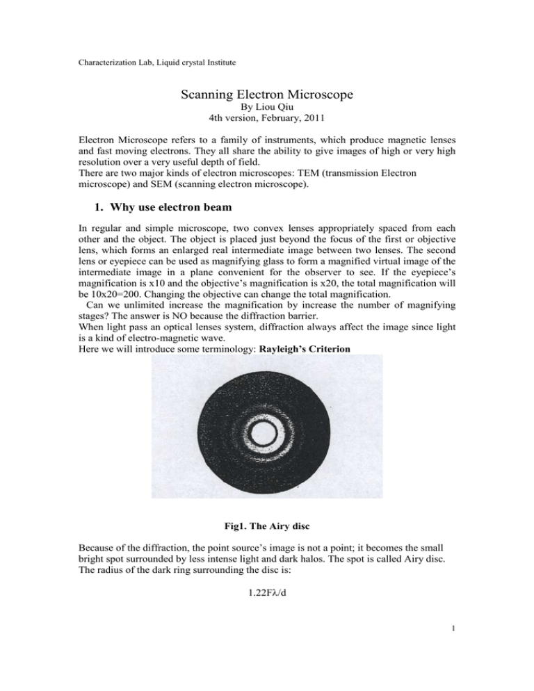
Characterization Lab, Liquid crystal Institute Scanning Electron Microscope By Liou Qiu 4th version, February, 2011 Electron Microscope refers to a family of instruments, which produce magnetic lenses and fast moving electrons. They all share the ability to give images of high or very high resolution over a very useful depth of field. There are two major kinds of electron microscopes: TEM (transmission Electron microscope) and SEM (scanning electron microscope). 1. Why use electron beam In regular and simple microscope, two convex lenses appropriately spaced from each other and the object. The object is placed just beyond the focus of the first or objective lens, which forms an enlarged real intermediate image between two lenses. The second lens or eyepiece can be used as magnifying glass to form a magnified virtual image of the intermediate image in a plane convenient for the observer to see. If the eyepiece’s magnification is x10 and the objective’s magnification is x20, the total magnification will be 10x20=200. Changing the objective can change the total magnification. Can we unlimited increase the magnification by increase the number of magnifying stages? The answer is NO because the diffraction barrier. When light pass an optical lenses system, diffraction always affect the image since light is a kind of electro-magnetic wave. Here we will introduce some terminology: Rayleigh’s Criterion Fig1. The Airy disc Because of the diffraction, the point source’s image is not a point; it becomes the small bright spot surrounded by less intense light and dark halos. The spot is called Airy disc. The radius of the dark ring surrounding the disc is: 1.22Fλ/d 1 Characterization Lab, Liquid crystal Institute Where F is the focal length of the lens and d is the diameter of the aperture, λ is the wavelength of the light. . Fig.2 (a) shows the intensity distribution in image of point object formed by perfect lenses. (b) The images of two close points will overlap but still can be distinguished until the pattern is too close to resolve. Fig.2 Intensity distribution of two adjacent image spots Refer to Fig 2. When the intensity maximum of one pattern falls in the first intensity minimum of the other, i.e., the separation between the two peaks is 1.22Fλ/d. Any lesser separation would result in formation of a continuous blur. We call this the Rayleigh Criterion. 2 Characterization Lab, Liquid crystal Institute Abbe did further research on the microscope system. He stated that the minimum resolvable separation d0 in the object was given by: d0 = 0.61λ/ (nsinα) Where λ is the wavelength, α = half angle subtended by the objective at the object. n is the index in the space between object and objective lens. The product nsinα is called the numerical aperture (NA) According the above discussing, the resolving power will be limited by several factors and λ is the most important factor if we want to raise resolving power. 2. the dual personality of Electron, De Broglie wavelength De Broglie showed that a moving electron had a dual personality. It can be regarded either as a moving charged particle or s a radiation with associated wavelength. λ=h/mv Where λ is the De Broglie wavelength of the electrons;h is the Plank’s constant and m is the mass while v is the velocity of electrons. So if we use electron beam as an illuminant, the wavelength by calculation will be very short. λ =1.23/ (V) ½ Table1. De Bloglie wavelength and accelerating voltage 3 Characterization Lab, Liquid crystal Institute Fig.3 Comparison of light microscope (left) and transmission electron microscope 3. Magnetic lens and Electrostatic Lens An electron moving in a magnetic field experiences a force tending to change its direction of motion except when it traveling parallel to the field. The principle of a magnetic lens is illustrated in Fig4. This shows an electron entering the magnetic field in the gap between two hollow cylindrical magnets arranged with unlike poles facing one another. Those traveling cross the field will be deflected because the Lorenz force. The focusing action, resulting in the electron path cutting the axis, is accompanied by a circum-ferential motion, illustrated in fig.4, in practice the complete figure would be rotated about the axis of symmetry xx’. So that a parallel beam of electrons entering the lens would be focused to a point on the axis of the field. Electrons traveling along the axis would be moving parallel to the magnetic lines of force and would be undeflected in their passage through the line field. This mechanism makes the focus possible if we utilize a solenoid; altering the current in the coil can vary the focal length of the lens. Also there is possibility of making magnifying system of several lenses in series whose magnification can be varied continuously or in fixed steps over a wider range. electrostatic lens are merely used because its disadvantages. Fig.4 Electron travel in the field of solenoid 4 Characterization Lab, Liquid crystal Institute 4. How SEM collects information from the sample, the detector Fig.5 showed the wealth of information from the sample after the electron beam is focused at it. We can use few of these characters basically; secondary electrons were selected to characteristic the specimen. Secondary electron detector will be installed to the system. The X radiation from the sample can tell not only topography but also the information of elements composed the sample. It will need another detector to use characteristic X-ray. Fig.5 Information resulting from the interaction between the electron beam and the specimen Fig .6, SEM(right) uses electron probe to scan, TEM(left) does not 5 Characterization Lab, Liquid crystal Institute 5. How the SEM works Electro-optically, the SEM has little in common with the TEM apart from the use of an electron gun and a condenser lens system to produce a focused electron beam. In SEM, these two or three lenses are the only ones in the column, there are no lenses after the specimen but only electro collector. The basic principle of the SEM is illustrated schematically in Fig 0. The whole system works under vacuum condition of 10-4 to 10-7 mbar. The vacuum condition makes the electron emission and acceleration possible. The electron source is the electron gun on the top of the column. Electrons were emitted by thermal emission. In some other SEM, field emission is used. SEM does scanning. A very fine “probe” of electrons with energies up to 30kevs focused at the surface of the specimen in the microscope and scanned across it in a “Raster” or pattern of parallel lines. Re-emission of secondary electrons and reflection (backscattered) electrons from the sample surface carried the information of the specimen. The intensity of emission of both the secondary and backscattered electrons is very sensitive to the angle at which the electron beam strikes the surface, i.e. to topographical features on the specimen. The emitted electron current is collected and amplified; variations in the resulting signal strength as the electron probe is scanned across the specimen are used to vary the brightness of the ray of CRT that is scanned in synchronism with the probe. There is thus a direct positional correspondence between the beam scanning across the specimen and the fluorescent image on the cathode ray tube. The magnification actually controlled by the scanning size. The magnification is the ratio of CRT screen area to the specimen area being scanned. The smaller the scanned area, the larger the magnification. 6. Why the resolution can not reach the limit of De Boiglie wavelength, several aberrations of the electron microscope As shown in the previous section, λ =1.23/ (V) ½, where V is the voltage. This shows a 30keV electron has a wavelength of 0.007nm. With this short wavelength, theoretically we can obtain very high resolution! If we can raise the accelerating voltage up to 106 volt, the De Boiglie wavelength will be only 1 pm. Nowadays a top TEM can have a resolution of 0.1 nm (or lower); the SEM in our lab declared resolution about 20nm. Actually, for our mostly polymer samples, we only obtain resolution about 100nm. 6 Characterization Lab, Liquid crystal Institute Why? Because what the table showing us were the theoretical data. In the real world, to make such a powerful and precise instrument needs big efforts in manufacture. Here we are going to discuss some aberrations of the electron microscope They are: a. Spherical aberration b. Chromatic aberration c. Astigmatism d. Distortion a. Spherical aberration The two main factors determining the resolving power of a microscope system are spherical aberration and refraction in the first, or objective, lens. Both of these cause a point objective to be imaged as a disc instead of a point, the diameter of the disc being dependent on the angular aperture of the lens. Spherical aberration causes losing of sharpness. Fig.8.disc of confusion because of aberration of lens Fig. 8 shows the formation of disc of confusion because of spherical aberration of lens It causes by the fact that extreme rays making an angle α to the lens axis are focused closer to the lens than the paraxial rays, result in a disc instead of a point. This disc is not the disc caused by diffraction, but they are same to cost the resolution of the microscope, they are same to cause the blurring image. The solution of the spherical aberration is to use the electron beam as narrow as possible. Or use an aperture to thinner the beam. b. Chromatic aberration In electron optics the equivalent of color is the electron energy, and chromatic aberration is the lens defect which degrades the image whenever electrons in the beam cease to be monoenergetic. Then the electrons with different energy will focus on different point. The solution is to make stability of electron energy. So the stability required in electron energy will be 1 in 105 volts! c. Astigmatism 7 Characterization Lab, Liquid crystal Institute Fig.9. Astigmatism In electron optics the astigmatism is caused by the electron deflecting fields not being perfectly symmetrical about the lens axis so the lens has a different focal length in different orientation. In practice, however the the pole-piece of a magnetic lens are machined there will always be slight departure from circularity in the bore. There may also be slight inhomogeneity in the iron used for the pole pieces. These defects result in a lens whose focal length varies slightly around the lens axis. There is certain methods can be used to correct the astigmatism, Fig.6. shows the electrostatic and electromagnetic stigmator, simple rotate the 2 sets of magnets and adjust the current in the coils, one can compensate the slight symmetrical problems. In our SEM, stigmator will be used after focusing. Fig.10.Electrostatic and electromagnetic stigmator 8 Characterization Lab, Liquid crystal Institute d. Distortion There are basically two kind of distortion: pincushion or barrel distortion. Distortion usually found when the lenses are being operated at larger focal lengths than the optimum, i.e. at low magnifying powers. The solution is to use good operation condition. Fig.11. Distortion 7. Coating of the specimen The primary electron beam, amounting to between 10-12 and 10-6 amperes depending on the spot diameter, is brought to rest in the specimen in the scanning microscope. A certain fraction of this current is emitted in the opposite direction as secondary or backscattered electron current. The net difference between the two currents must be enabled to leak away to earth via the stub, or the specimen will charge up as a capacitor. The change in the specimen potential can be such as to influence the scanning beam and adversely affect the quality and resolution of the image. So it is required to make a conducting “skin”. Specimen coating, usually by vacuum deposition or sputtering is normally carried out on all insulating and semi-insulating material before they are examined in the SEM. In our lab the coating is made by sputtering. A gold ring with diameter 3 inch was installed on the top of a vacuum chamber. The specimens are laid on the bottom of the chamber facing the gold ring. Purge the chamber with Argon, vacuum the chamber into a certain miliTorr, then applied a DC voltage on the top and bottom electrodes. Electric discharge will happen under the certain vacuum degree. The ions in the discharge will run towards the cathode where the gold target is. Ions bombard the gold target and hit out gold atoms. The gold particles then deposit onto the specimen surface. The thickness of the gold coating for our experiment is about 40nm 9 Characterization Lab, Liquid crystal Institute Au, cathode ions Vacuum Chamber DC Pules Au Au specimen Fig.12, Use sputtering to make the specimen surface conductive Procedure of the experiment. 1. Students are required to prepare the sample, Do sputtering. 2. Under the instruction of the lab instructor, learn the basics to operate the SEM: Install sample, turn on the high voltage with filament current; learn how to find the optimum working condition, focus and magnification. 10 Characterization Lab, Liquid crystal Institute Procedure of Sputtering 1. Prepare sample. Use conductive tape to stick the sample on the sample stub, label the stub. 2. Use silvers paste to paste the sample edge. 3. (Optional: Put the sample into an oven with Temperature of 105°c for 110 min to cure the silver paste...) 4. Put the samples into the chamber of the sputter. 5. Open the top valve of Argon tank the regulator show out put pressure is 5psi. 6. Close the needle valve on the panel. 7. Turn on the vacuum, press the cap of the chamber for few seconds to help. 8. Wait till the vacuum meter show it pump down to 40miliTorr, open the needle valve for Argon, pressure becomes >100militorr, close valve again, repeat 3 times to purge the chamber. 9. Adjust the valve to keep the vacuum 60-70miliTorr. 10. Adjust the timer between 2-3 min, select Auto. 11. Turn the Pulse On, turn on the voltage till current reach 10mA DC on the meter. Sputtering starts under discharge during the time preset. 12. After sputtering, turn voltage to 0 then off, auto to manual. 13. Push the vacuum button to turn off the vacuum. 14. Turn off the top valve of Ar tank. 15. Wait 1 min, open the chamber cape, and take off the sample. Procedure of SEM, Please see attached lab procedure Basic Procedure of operating Hitachi S-2600N By Liou Qiu Feb.9, 2006 1. Click on PS-SEM_XONE to open the software. 2. Make sure the high voltage was off , then press the button of Air/Evac to vent the chamber 3. Wear a vinyl glove, screw the sample stub onto the screw, and push the screw into the socket of sample holder at the center of the specimen chamber. 4. Close the door of the chamber, press the button of Air/Evac again to vacuum the system, wait till the vacuum indicator on the screen turns light green then blue. 5. Turn on the High Voltage by click on the high voltage tab on the screen( the tab frame becomes red), adjust the Beam size to about 25-30 usually, adjust “Z” knob to adjust the Working Distance(WD) to briefly focus the sample, then use the knob of “focus” to do the fine focus till see the optimum. 11 Characterization Lab, Liquid crystal Institute 6. Adjust X, Y knobs to find right spot that you are interested in., adjust the” “Contrast” and “Brightness” till optimized image. 7. Increase the Magnification to your desire, fine focus again. You can use reduced image or various scan rate when focus the image. 8. Adjust the Stigmator/Alignment till optimum image obtained 9. Once you get a satisfied image, capture the image by click the tab “M”. 10. After several images were taken for one sample, you can turn off the high voltage by press the tab " High Voltage”, the image area must turn black now. 11. Vent the chamber then to take out the sample. 12. Press the tab of “Captured Images” to see the images. 13. Press files- descend to sort the images. 14. Select the images you like to save and save in proper folds. press the tab of “Batch saving” and input the filename, click ‘Ok’ 15 You files are thus saved, please use “Convert” to convert them into JPG files if you like. (Usually we select the high voltage at 20kv, select beam size about 25, WD about 15mm. It depends on the experiment needs, the voltage can be 5kv-30kv, the minimum WD is 5mm, the beam size may vary from 3-100. When doing energy dispersive X-ray spectrum, select larger beam spot to match the requirement of counting rate) 12 Characterization Lab, Liquid crystal Institute Fig.0, Scanning Electron Microscope of Jeol 13


