AMMP-XXXX
Production Assembly Process
Application Note 5386
Description
Package Features
This application note describes and illustrates the attachment and detachment of Avago’s 5x5 mm packaged
products in a PCB (soft board) environment. The AMMP
package has a solid copper filled cavity to allow optimum
thermal transfer of the packaged device to the PCB and
associated heat sink interface.
• Surface Mount Package (5x5 x 1.25 mm)
• Tape and reel capability for chip shooter pick-and-place
applications.
1 2
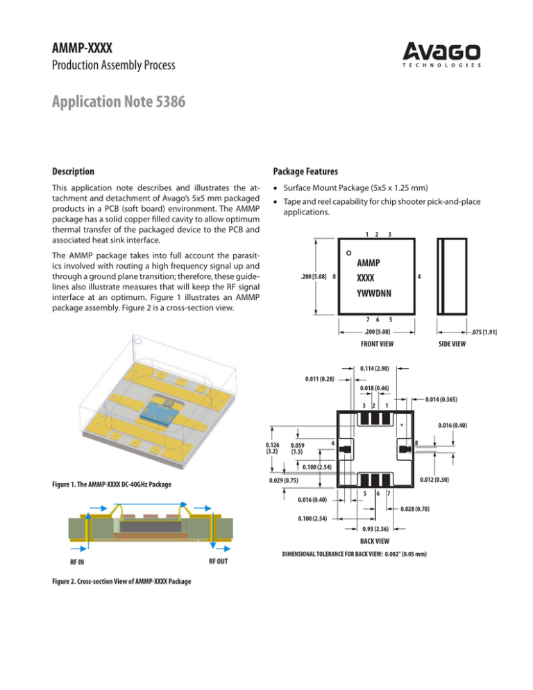
The AMMP package takes into full account the parasitics involved with routing a high frequency signal up and
through a ground plane transition; therefore, these guidelines also illustrate measures that will keep the RF signal
interface at an optimum. Figure 1 illustrates an AMMP
package assembly. Figure 2 is a cross-section view.
.200 [5.08] 8
3
AMMP
XXXX
YWWDNN
7 6
4
5
.200 [5.08]
.075 [1.91]
FRONT VIEW
SIDE VIEW
0.114 (2.90)
0.011 (0.28)
0.018 (0.46)
3 2
0.014 (0.365)
1
0.016 (0.40)
*
0.126
(3.2)
0.059
(1.5)
8
4
0.100 (2.54)
0.012 (0.30)
0.029 (0.75)
Figure 1. The AMMP-XXXX DC-40GHz Package
0.016 (0.40)
5
6
7
0.028 (0.70)
0.100 (2.54)
0.93 (2.36)
BACK VIEW
RF IN
Figure 2. Cross-section View of AMMP-XXXX Package
RF OUT
DIMENSIONAL TOLERANCE FOR BACK VIEW: 0.002" (0.05 mm)
Package Dimension Tolerances
Stencil Type
A stainless steel stencil with trapezoidal walls is recommended. If possible, electropolishing for smooth walls will
reduce surface friction and promote good paste release.
The trapezoidal section aperature (TSA) design also promotes precision solder deposits to assist in component
placement and alignment. The resulting, reflowed solder
joints on the perimeter I/O lands should measure approximately 50 µm to 75µm (2 to 3 mils) standoff height. Figure 3 is a drawing for a stencil pattern that optimizes the
amount of solder paste that maximizes contact coverage
and minimizes thickness, which would degrade RF signal
performance.
1.47
1.04
2.49
0.56
0.25
0.15
2.79
0.36
0.77
0.38
0.72
Figure 4. Epoxy Pattern on PCB
Manual Solder Dispension Guidelines
For manual dispension of solder paste on the PCB, it is
critical to distribute the solder paste evenly in the same
pattern as shown in Figure 4 above. The amount should
be distributed in an even pattern at a thickness of approximately 0.1 mm (0.004”), because when solder is unevenly
distributed it may result in voids underneath the package
or non-contact on parts of the package bottom. Too much
solder paste may result in bridging of the contact pads.
Figure 5 illustrates possible conditions that may occur
with poor distribution of solder paste.
0.1
0.39
0.55
0.52
0.3
Figure 3. Solder Stencil Dimensions
Solder Paste
AMMP mounted with good distribution
of solder under contact pad area.
Recommended solder paste is SolderPlus 62NCLR-A/Sn62
Pb36 Ag2 (Engineered Fluid Dispensing). Details can be
obtained from http://www.efd-inc.com
If the vias on the PCB are not silver filled, taping the backside of the PCB with thermal tape, prior to dispensing the
solder paste, is recommended.
void
AMMP mounted with too much solder
in center pad area.
This will help containment of the solder in the vias which
is critical for proper thermal transfer from the package to
the PCB and heat sink. Remove thermal tape after the cool
down period of the solder process.
If lead-free solder is required, a “no clean” Type 3 paste per
ANSI/J-STD-005 is recommended. Nitrogen purge is also
recommended during reflow.
For automated assembly, solder paste should be screen
printed before reflow. Figure 4 illustrates the solder deposit pattern superimposed on the PCB.
2
void
AMMP mounted with too little solder in
center pad area. (Void exists resulting
in poor thermal transfer)
Figure 5. Solder Dispension Illustrations
PCB Land Pattern and Material
Profile for Solder Reflow
The PCB material and mounting pattern, as defined in
the data sheet, optimizes RF performance and is strongly
recommended. An electronic drawing of the land pattern
is available upon request from Avago Sales and Application Engineering. Figure 6 is a drawing of the land pattern. Material is Rogers RO4350 with thickness of 0.25 mm
(0.010”).
The reflow profile investigated and recommended by
Avago for this product is based on JEDEC/IPC standard
J-STD-020 revision C. This device has been qualified to
withstand a maximum of three cycles of solder reflow
according to the conditions of J-SDT-020C, and this device has been qualified for moisture sensitivity level 2a.
Figure 7 depicts this standard lead-free JEDEC/IPC profile.
Table 1 lists the parameters and peak temperatures as
indicated by JEDEC/IPC. The most recommended and
most common reflow method is accomplished in a belt
furnace using convection/ IR heat transfer.
For products with approximately 2 W dissipation or greater, silver filled vias are highly recommended.
.093 [2.36]
.010 [0.25]
.011 [0.28]
.016 [0.40]
.0095 [0.24]
.020 [0.50]
.016 [0.04]
.126 [3.20]
.059 [1.50]
.012 [0.3]
.018 [0.46]
.0095 [0.24]
.018 [0.46]
.114 [2.90]
Figure 6. AMMP-XXXX Land Pattern
Solder Reflow
Reliable assembly of surface mount components is a complex process that involves many material, processes, and
equipment factors, including: method of heating, circuit
board material, conductor thickness, pattern, type of
solder paste and solder alloy, thermal conductivity, and
thermal loading and mass of components. Reflow temperature settings need to be determined by the user
based on these considerations. Also, moisture sensitivity
level (MSL) 2A has been qualified for this device. The MSL
2A conditions must not be exceeded.
After ramping up from room temperature, the circuit board
with components held in place with solder paste, passes
through one or more preheat zones. The preheat zones increase the temperature of the board and components to
prevent thermal shock and evaporation of solvents from
the solder paste. The reflow zone briefly elevates the temperature sufficiently to produce a reflow of the solder.
3
Table 1 shows the actual temperature range that should
occur on the surface of a test board at or near a central solder joint. During this type of reflow soldering, the circuit
board and solder joints tend to heat first. The components
on the board are then heated by conduction. The circuit
board, because it has a large surface area, absorbs thermal
energy more efficiently, then distributes this heat to the
components.
Do not uses prolonged hot preheat due to excessive
oxidation which can occur on the solder powder surface.
The time at peak is not critical and usually not measured
as it is very dependent upon the type of oven used. However, time over 217° C is critical and will determine the
appearance of the solder joint after reflow. Longer reflow
time may result in dull and gritty solder joint appearance
and charring of flux residues. Time below 30 seconds may
result in insufficient wetting and poor intermetallic formation. Too fast of a cooling rate could result in insufficient
wetting and poor intermetallic formation.
As a general guideline, this package should be exposed
to only the minimum lead-free process temperature and
times necessary to achieve a uniform reflow of solder on
the board. The rates of change of temperature for the
ramp-up and cool-down zones are specified by J-STD020C standard to be low enough to not cause deformation of the board or damage to components due to thermal shock. This profile allows a reflow temperature which
is low enough to avoid damaging the internal circuitry
during solder reflow operations provided the time of
exposure at peak reflow temperature is not excessive.
Also refer to the AMMP-XXXX product data sheet for
further information.
Table 1. Typical SMT Reflow Profile for Maximum Temperature = 260+0 / -5° C
Profile Feature
Sn-Pb Solder
Pb-Free Solder
Average ramp-up rate (TL to TP)
3° C/sec max
3° C/sec max
Preheat
– Temperature Min (Tsmin)
– Temperature Max (Tsmax)
– Time (min to max) (ts)
100° C
150° C
60-120 sec
150° C
200° C
60-180 sec
Tsmax to TL
– Ramp-up Rate
3° C /sec max
Time maintained above:
– Temperature (TL)
– Time (TL)
183° C
60-150 sec
217° C
60-150 sec
Peak temperature (Tp)
240 +0/-5° C
260 +0/-5° C
Time within 5° C of actual Peak Temperature (tp)
10-30 sec
20-40 sec
Ramp-down Rate
6° C /sec max
6° C /sec max
Time 25° C to Peak Temperature
6 min max.
8 min max.
tp
Tp
Critical Zone
TL to Tp
Ramp-up
Temperature
TL
tL
Ts max
Ts min
Ramp-down
ts
Preheat
25
t 25°C to Peak
Time
Figure 7. Standard J-STD-020C Lead-free Solder Reflow Profile.
4
Desoldering the AMMP Package
Desoldering can be done by hot-air, hot-tip contact and on
a hot plate. An example of hot-plate desoldering is shown
in Figure 8. An aluminum block, sized to fit under the 5x5
mm package area, is used to transfer the heat from the
hot plate. The aluminum block centralizes the heat under
the package and avoids reflow of surrounding components. When the solder has reflowed, the package should
be removed by gripping it with tweezers from the bottom
section. Figure 9 shows various blocks, a typical hot plate
set to approximately 200° C and an AMMP PCB assembly.
Figures 10 and 11 show the removal of the AMMP package using tweezers.
Package Top
Package Bottom
AMMP PCB assembly on
top of aluminum block
PACKAGE
PCB
Aluminum Block
Hot Plate
Figure 8. Hot Plate Desoldering
Figure 10. AMMP on Aluminum Block
Gold plated
copper block
AMM
Aluminum block
Figure 9. Typical Hot Plate and Components
Figure 11. Removal of AMMP Package
5
Hot Air Desoldering
Figure 14 shows an illustration of blowing hot air underneath the demostration board by using the hot air nozzle
and at the same time using tweezers to grip the bottom
side walls of the AMMP package.
Hot Air Equipment
HAKKO FM202
Nozzle: A1130
Figure 14. Blowing Hot Air Underneath the Demostration Board
Figure 12. AMMP-XXXX Soldered on PCB
Figure 13. PCB Secured for Access Underneath PCB
6
Hot Tip Contact Desoldering
Hot Tip Equipment
HAKKO 850D
PACKAGE TOP
PACKAGE
PACKAGE BOTTOM
PCB
COPPER HEATSINK
Direct contact is made under
the package surface area.
PACKAGE TOP
PACKAGE BOTTOM
PCB
PACKAGE
Lift package, with tweezers, from
bottom side walls when solder has
reflowed, as shown in Figure 14.
COPPER HEATSINK
Keep direct contact under the package
surface area to reflow solder.
Figure 15. Hot Tip Desoldering
7
Special Handling Notes for Automatic and Manual SMT
Rework
• Package should be cooled down before any solution
cleaning after IR reflow.
AMMP
AMMP
XXXX
XXXX
YWWDNN
YWWDNN
• Solder coverage should be evenly distributed across
the bottom contact area to obtain good, reliable DC
and RF contact.
• Alignment and good wetting of the RF In/Out pad to the
PCB is critical to ensure optimum signal transmission.
• Handling the package along the edges with tweezers
or auto placing with vacuum force from the top of the
lid is recommended.
5.08 mm
• DC probe or other sharp instrument contact is
prohibited in the bottom center area outlined in Figure
16. DC probe contact or other sharp instrument contact
is allowed in the area marked “A”.
• For volume production, the AMMP package can be
treated as a standard surface mount component
(ref. IPC/JEDEC J-STD-020C std. or equivalent) with a
standard assembly process. (eg, stencil solder printing,
standard pick and place, and solder reflow oven).
AA
RF IN
NoNo
direct
direct
probing
allowed
probing
allowed
onon
this
area.
this
area.
A
Figure 16. Prohibited Probing Area
8
5.08 mm
AA
RF Port Transitions
Manufacturer URL:
It is important to note that RF port hardware, such as SMA
2.92 mm or 2.4 mm connectors, will directly contribute
loss and limit the AMMP performance within the hardware’s bandwidth.
http://www.southwestmicrowave.com
Table 2 is a list of recommended edge launch connectors, used in Avago’s mmWave evaluation board modules.
Other connectors with similar performance will also be
suitable.
Bypass capacitors, as recommended at the DC pin outs on
Avago AMMP data sheets, should be as close to the package as possible. Table 3 lists two typical values and their
part numbers. Other capacitors similar in specification
may be substituted.
http://www.EmersonNetworkPower.com
Bypass Capacitors
Table 2. Recommended Edge Launch Connectors
Connector Type
Bandwidth
Manufacturer
Female Part Number
Male Part Number
SMA (screw on)
DC-27GHz
Southwest Microwave
292-06A-5
293-03A-5
SMA (solderable)
DC-26.5GHz
Johnson
142-0761-841-A
SMA (solderable)
DC-26.5GHz
Johnson
142-0761-851-A
SMA (solderable)
DC-26.5GHz
Johnson
142-0761-891-A
2.92 mm (screw on)
DC-40GHz
Southwest Microwave
1092-04A-5
1092-03A-5
2.4 mm (screw on)
DC-50GHz
Southwest Microwave
1492-03A-5
1493-03A-5
Table 3. Bypass Capacitors
Capacitor Type
Value
Manufacturer
Part Number
SMT 0402
0.1 mF
AVX
AVX0402YG104ZAT2A
SMT-0805
>1 mF (4.7 mF)
Phycomp
08052F47SZ6BBOD
For product information and a complete list of distributors, please go to our web site:
www.avagotech.com
Avago, Avago Technologies, and the A logo are trademarks of Avago Technologies in the United States and other countries.
Data subject to change. Copyright © 2005-2010 Avago Technologies. All rights reserved.
AV02-1245EN - August 27, 2010


