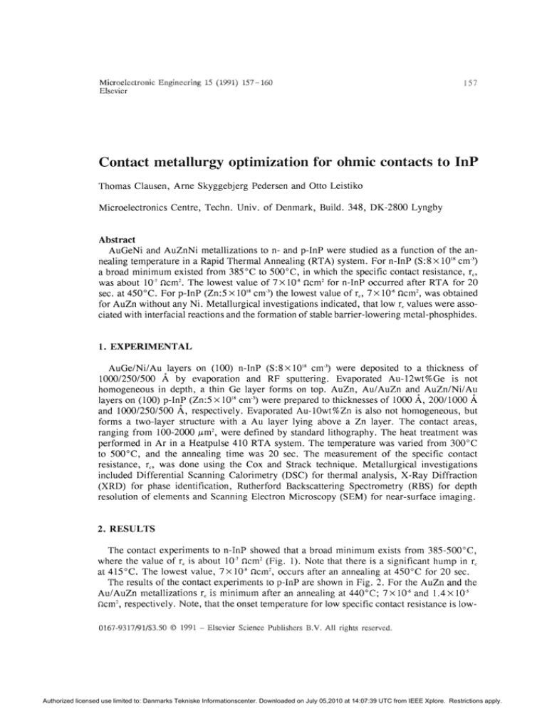
Microelectronic
Elsevier
Engineering 15 (1991)
Contact metallurgy
Thomas
157-160
optimization for ohmic contacts to InP
Clausen, Ame Skyggebjerg Pedersen and Otto Leistiko
Microelectronics Centre, Techn. Univ. of Denmark, Build. 348, DK-2800
Lyngby
Abstract
AuGeNi and AuZnNi metallizations to n- and p-InP were studied as a function of the an¬
nealing temperature in a Rapid Thermal Annealing (RTA) system. For n-InP (S:8x IO18 cm"3)
a broad minimum existed from 385°C to 500°C, in which the specific contact resistance, rc5
was about IO"7 Ocm2. The lowest value of 7x IO'8 flcm2 for n-InP occurred after RTA for 20
sec. at 450°C. For p-InP (Zn:5 x IO18 cm"3) the lowest value of rc, 7x IO"6 ncm2, was obtained
for AuZn without any Ni. Metallurgical investigations indicated, that low rc values were asso¬
ciated with interfacial reactions and the formation of stable barrier-lowering metal-phosphides.
1. EXPERIMENTAL
AuGe/Ni/Au layers on (100) n-InP (S:8xl0!8 cm"3) were deposited to a thickness of
1000/250/500 Á by evaporation and RF sputtering. Evaporated Au-12wt%Ge is not
homogeneous in depth, a thin Ge layer forms on top. AuZn, Au/AuZn and AuZn/Ni/Au
layers on (100) p-InP (Zn:5 x IO18 cm"3) were prepared to thicknesses of 1000 À, 200/1000 Á
and 1000/250/500 A, respectively. Evaporated Au-10wt%Zn is also not homogeneous, but
forms a two-layer structure with a Au layer lying above a Zn layer. The contact areas,
ranging from 100-2000 /im2, were defined by standard lithography. The heat treatment was
performed in Ar in a Heatpulse 410 RTA system. The temperature was varied from 300°C
to 500°C, and the annealing time was 20 sec. The measurement of the specific contact
resistance, rc, was done using the Cox and Strack technique. Metallurgical investigations
included Differential Scanning Calorimetry (DSC) for thermal analysis, X-Ray Diffraction
(XRD) for phase identification, Rutherford Backscattering Spectrometry (RBS) for depth
resolution of elements and Scanning Electron Microscopy (SEM) for near-surface imaging.
2. RESULTS
The contact experiments to n-MP showed that a broad minimum exists from 385-500°C,
where the value of rc is about IO"7 Ocm2 (Fig. 1). Note that there is a significant hump in rc
at 415°C. The lowest value, 7x10"8 Ocm2, occurs after an annealing at 450°C for 20 sec.
The results of the contact experiments to p-InP are shown in Fig. 2. For the AuZn and the
Au/AuZn metallizations rc is minimum after an annealing at 440°C; 7 x10"6 and 1.4 x10"5
Ocm2, respectively. Note, that the onset temperature for low specific contact resistance is low-
0167^9317/91/13.50 © 1991
Elsevier Science Publishers B.V. Ali
rights reserved.
Authorized licensed use limited to: Danmarks Tekniske Informationscenter. Downloaded on July 05,2010 at 14:07:39 UTC from IEEE Xplore. Restrictions apply.
,58
T. Clausen et al
/ Contact metallurgy optimization
10 % rc(Qoiif
li) "4;
AuGe/Ni/Au
10 "5!
10 ~6i
10 '7\
Temp.(°C)
10
300 350 400 450 500
Fig.
1. rc
vs.
AuZn
Au/AuZn
AuZn/Ni/Au
350
ann.temp, for AuGeNi/n-InP. Fig. 2.
rc
vs.
Temp.(°C)
400
450
500
ann.temp, for AuZn(Ni)/p-InP.
ered by adding the Au layer below the AuZn. However, the lowest obtainable specific contact
resistance for the Au/AuZn layer is two times larger than for the AuZn layer alone. From
Fig. 2 it is also seen, that the addition of Ni alters the temperature dependence of rc quite
drastically. Below 425°C rc is lower than for the AuZn layer alone, but again, as for the
AuGeNi/n-InP system, there is a hump at 415°C The rc minimum 2.7xl0"5 ncm2 occurs at
430°C. Above 430°C rc increases abruptly to about IO3 ncm2.
The metallurgical investigations showed, that the onset of low values of rc were associated
with interfacial reactions between the InP and the AuGeNi or AuZn(Ni), respectively. Exam¬
ples of this are shown in Fig. 3 and 4, where RBS plots and SEM pictures of AuGeNi and
AuZn reactions with InP are shown. The as-deposited layers were smooth and uniform (SEM)
and there was no intermixing of the elements (RBS). From DSC of the AuGeNi/InP structure
two independent and overlapping exothermic peaks ranging from 200-260 °C and 240-370 °C
were identified. The termination of the last peak and the onset of minimum rc coincides quite
well. For AuZn, the Zn redistributes below 400°C because of the low heating rate of the ap¬
plied DSC instrument (50°C/min. compared to 100°C/sec. of the RTA system), and therefore
a DSC experiment involving AuZn will be incorrect in determining the onset temperature for
RTA reactions. By XRD various Au-In phases were identified: At 440-450°C annealing a
pink Au3In phase formed (Fig. 4a) and at 465°C a combination of Au3In and Aujn^ At
500°C annealing an eutectic melting of Auln and Auln2 was detected (Fig. 4b).
.
3. DISCUSSION
It is apparent from the electrical characterization, that rc exhibits an overall minimum for
both AuGeNi, AuZn and Au/AuZn around 440-450°C, while for the AuZnNi system there
is an abrupt increase in rc around 440°C. In this section the role of the metallization elements
are
discussed
individually.
The role of Au
Au is perhaps the most important element to be discussed, since this is the element that
governs the degradation of InP most extensively. Many authors have studied the Au-InP sys¬
tem13, and a general path in the degradation process may be constructed. Up to 12.7 at % In
is soluble in Au» and this Au(In) solution is the first step in the process. The next step is the
Authorized licensed use limited to: Danmarks Tekniske Informationscenter. Downloaded on July 05,2010 at 14:07:39 UTC from IEEE Xplore. Restrictions apply.
T. Clausen et al.
/ Contact metallurgy optimization
1500^ Yield
loOOi Yield
1000
AuGe/Ni/Au,* J
500
As-dep
°C
350
450 °C
Fig.
1000 AuZn
500^
100 200 300 400 500
Channel no.
0
3. RBS
plots
159
a)
of a) AuGeNi/n-InP and
10i«i25.8kU 5.0BE3 1766/01 458 C
0
0
b) AuZn/p-InP
As-dep
°C
400
430 °C
100 200 300 400 500
Channel no.
reactions.
b)
5.B8E3 lSBB'Bl
T5
Fig. 4. SEM-picture of a) AuGeNi/n-InP annealed at 450°C for 20 sec. and of b) AuZn/p-InP
annealed at 500°C for 20
sec.
formation of Au-In phases. Referring to the Au-In binary system' and the Au-In-P ternary
system2 these are the e- and y-phases (Au3In and Au,In4). Further degradation leads to higherorder Au-In phases, but there is some uncertainty about the next phases to be formed. We
have detected a Auln-Auln2 eutectic melting at 500°C, with no other Au-In phases present be¬
tween this and the y-phase. Au and P can only form one phase, the metastable Au2P3. Forma¬
tion of both Au-In phases and Au2P3 only occurs, when the e-phase is formed. For other AuIn phases, P either evaporates or is left at the interface between the metals and the InP3.
The lowest rc for n- and p-InP (430-450°C annealing) coincides with a poor morphology
and growth of Au3In. In order to improve this morphology, it is an advantage to involve a
melting of the Au3In phase (TM"RÍ4950C). A better morphology is also expected to lower rc
even further. Therefore an experiment was made in which Au3In was grown at 370°C in a
conventionel oven and subsequently melted in the RTA system at 500°C for a few seconds.
Due to some uncertainty in the annealing time required for growing the Au3In 20, 40 and 90
min. were tested. Annealing for 40 min. gave the lowest rc value, 5 x IO8 ncm2, and an almost
total coverage of the pink Au3In phase.
Authorized licensed use limited to: Danmarks Tekniske Informationscenter. Downloaded on July 05,2010 at 14:07:39 UTC from IEEE Xplore. Restrictions apply.
160
T. Clausen et al
/ Contact metallurgy optimization
The role úf Ge and Zn
Ge and Zn are generally assumed to act as donors and acceptors, respectively, in InP, and
they are thought to replace Ii in the lattice. Various authors have shown the formation of
compounds involving Ge or Zn adjacent to the InP surface. For Ge, a ternary AuGeP phase
is observed5, and it is shown that this phase actually lowers the barrier height to 0,15 eV. Zn
is shown to react with P, creating ZnP phases4, but there is no information on the electronic
properties of these compounds with respect to p-InP.
The role of Ni
Ni is important in obtaining low values of rc for n-InP (Fig. 1), but for p-InP (Fig. 2) the
use of Ni causes an abrupt increase in rc at 440°C. For a AuZn structure without Ni, rc is mi¬
nimum at this temperature. Thus, it seems that the electronic properties at the interface chan¬
ges, and that the changes are associated with phase formations. It has been shown5"7, that free
Ni diffuses through the Au(Ge/Zn) layer to the InP surface, where Ni(Ge/Zn)P phases eventu¬
ally form. These MP phases, associated with the exothermic peak from 240-370°C, are re¬
sponsible for the changes in the electronic properties8,9. For n-InP the barrier height decreases
to 0.1+0.1 eV when NiP phases are formed8,9, while the barrier height for p-InP increases.
This partly explains the appearance of the curves in Fig. 2. rc is lower for Ni containing
contacts below 425°C for p-InP, because Ni lowers the reaction temperature. The hump at
415°C for both AuZnNi and AuGeNi contacts to InP are propably associated with two diffe¬
rent phase formation regimes due to the addition of Ni. In the first regime, Ni reactions
govern the value of rc. In the second regime, reactions between Au and InP preferentially oc¬
cur, creating first the Au(In) solution with less P for Ni-P or Zn-P reactions and later Au3In
with more P adjacent to the InP surface for Ni-P or Zn-P reactions.
4. CONCLUSION
The formation of a Au3In phase during annealing is essential for obtaining low-resistance
ohmic contacts to both n- and p-InP using conventional AuGeNi and AuZn metallization
schemes. By growing this phase, a considerable amount of phosphorous will be present at the
interface between the metallization and the InP for energetically favorable reactions with Ge,
Ni, NiGe and AuGe for n-InP and with Zn or AuZn for p-InP. These metal-phosphides, being
thermodynamically stable, lowers the Schottky barrier height, normally believed to be pinned
at a certain value, and ensures excellent low-resistance ohmic contacts.
5- REFERENCES
1 A. Prince, Phase diagrams of ternary gold alloys, The Institute of Metals, 1990.
2 C.T. Tsai and R.S. Williams, J. Mater. Res., 1(6) (1986) 820.
3 V.G. Weizer and N.S. Fatemi, J. Appl. Phys., 68(5) (1990) 2275.
4 O. Oparaku, Semicond. Sei. TechnoL, 5 (1990) 65.
5 RJ. Graham and J.W. Steeds, lest. Phys. Conf. Ser. No. 67 (1983) 507.
6 J.A. del Alamo and T. Mizutani, Solid^State Electronics, 31(11) (1988) 1635.
7 LB. Boos and W. Kruppa, J. Vac. Sei. Technol., B7(3) (1989) 502,
8 A. Appelbaum, IEEE Trans. Eiec* Dev,, ED-34(5) (1987) 1026,
9 L.T BriJJson, Appl. Phys. Lett., 38(10} (1981) 284,
Authorized licensed use limited to: Danmarks Tekniske Informationscenter. Downloaded on July 05,2010 at 14:07:39 UTC from IEEE Xplore. Restrictions apply.


