MWF Lecture 23
advertisement
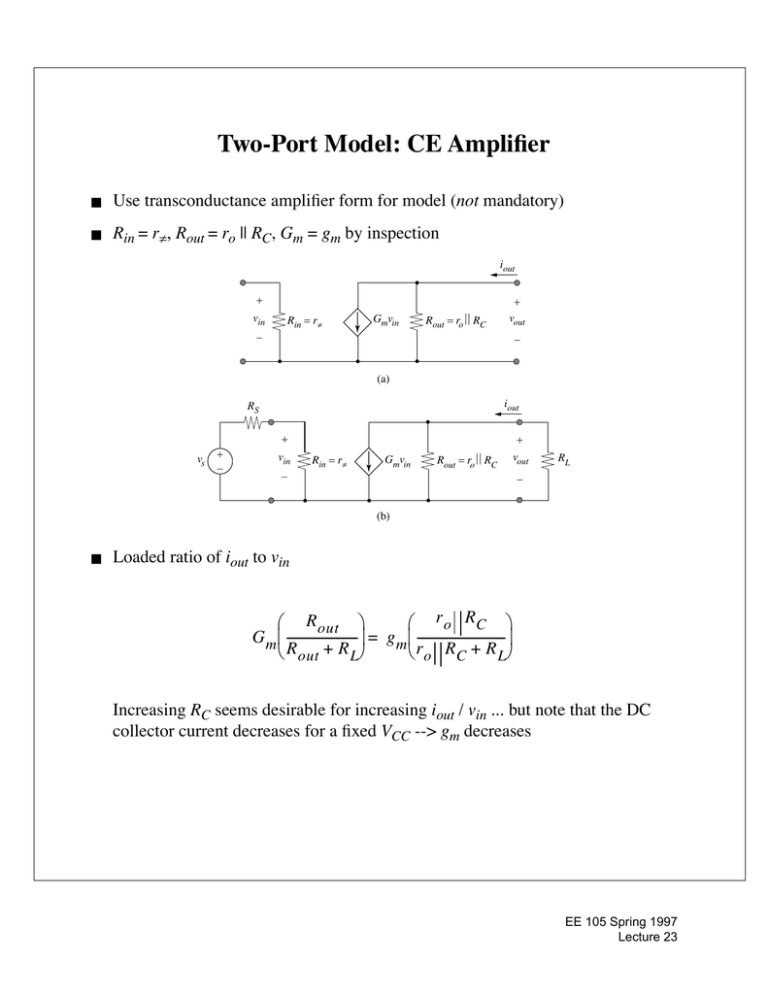
Two-Port Model: CE AmpliÞer ■ Use transconductance ampliÞer form for model (not mandatory) ■ Rin = rπ, Rout = ro || RC, Gm = gm by inspection iout + vin _ Rin = rπ Gmvin Rout = ro RC + vout − (a) iout RS + vs + − vin _ + Rin = rπ Gmvin Rout = ro RC vout RL − (b) ■ Loaded ratio of iout to vin R out ro RC G m ------------------------ = g m ------------------------------ R out + R L r o R C + R L Increasing RC seems desirable for increasing iout / vin ... but note that the DC collector current decreases for a Þxed VCC --> gm decreases EE 105 Spring 1997 Lecture 23 Common-Source AmpliÞer ■ ConÞguration is similar to common-emitter VDD VDD RD RD iOUT = IOUT + iout RS vs VBIAS + + − vOUT = VOUT + vout RL − + − (a) ■ VBIAS + VOUT _ + − (b) Bias: remove source and load resistances (b) EE 105 Spring 1997 Lecture 23 Graphical Load-Line Analysis ■ Load line is given by: I D = ( V DD Ð V OUT ) ⁄ R D ID (mA) 1.0 4 0.9 VBIAS (V) 0.5 4 3 3 0.25 2.5 2 0.10 0 VBIAS ≤ VTn = 1 V 2 1 1 2 3 4 5 VDS = VOUT (V) (a) VOUT HighGain Region 5V 1 2 3 4 2.5 V VBIAS (b) EE 105 Spring 1997 Lecture 23 Small-Signal Model of CS AmpliÞer ■ Substitute parameters at operating point selected so that V OUT ≈ V DD ⁄ 2 iout + + vgs gmvgs ro RD vout − − (a) iout RS + vs + − vgs gmvgs ro RD RL + vout − − (b) Transconductance is proportional to ID1/2 unlike bipolar transistor EE 105 Spring 1997 Lecture 23 Two-Port Model of Common-Source AmpliÞer ■ Use transconductance ampliÞer form for model (most natural choice) Rin = inÞnty, Rout = ro || RD, Gm = gm by inspection iout + vin + Gmvin Rout = ro RD vout − − (a) iout RS + vs + − vin + Gmvin Rout = ro RD vout − RL − (b) InÞnite input resistance is ideal for a voltage input Output resistance increases with RD increasing, but DC drain current ID will decrease and gm will decrease with ID1/2 EE 105 Spring 1997 Lecture 23 Current-Source Supplies ■ A current source to supply current, rather than a resistor, allows a high DC current for the device with a large incremental (small-signal) resistance iSUP + + vSUP vSUP iSUP − roc ISUP − (a) iSUP 1 roc ISUP roc vSUP (b) (c) EE 105 Spring 1997 Lecture 23 Common-Source with Current Source Supply ■ RD is replaced with idealized current source with internal resistance VDD VDD iSUP ISUP iOUT = IOUT + iout + RS vs VBIAS vOUT = VOUT + vout + − − + − (a) ■ + VOUT RL VBIAS + − − (b) For DC bias analysis, the small-signal source (with RS) and the load resistor RL are eliminated, along with the internal resistance roc of the current source EE 105 Spring 1997 Lecture 23 Graphical Analysis of CS AmpliÞer with Current-Source Supply ID (mA) 1.0 4V 0.9 VBIAS 0.5 3V 0.25 2 3 4 2.5 V 2V 0.10 0 VBIAS ≤ VTn = 1 V 1 1 2 3 4 5 VDS = VOUT (V) (a) HighGain Region VDD 1 2 3 4 0 0 2.5 V VBIAS (b) ■ The region of input bias voltage VBIAS for which the current source and the MOSFET are in their constant-current regions is extremely small .... EE 105 Spring 1997 Lecture 23 Common-Source/Current-Source Supply Models ■ The small-signal model is identical to the resistor supply, except that the current sourceÕs internal resistance roc replaces RD iout + + vgs gmvgs ro roc vout − ■ − Two-port model in both transconductance and voltage ampliÞer forms (the latter by direct conversion from the former ... by applying procedure for Þnding Av) iout + vin Gmvin − (a) Rout iout Rout + vin − + − Avvin = −GmRoutvin + vout − (b) EE 105 Spring 1997 Lecture 23 p-Channel Common-Source AmpliÞer ■ Source of p-channel is tied to positive supply; current supply sinks ISUP to ground or to lower supply VDD VDD RS vs + − VBIAS + − iOUT = IOUT + iout VBIAS + vOUT = VOUT + vout iSUP + − RL _ (a) ■ ISUP + VOUT _ (b) Small-signal model: substitute p-channel model directly EE 105 Spring 1997 Lecture 23 p-Channel CS Small-Signal Model ■ Source is at top, but circuit can be inverted to show correspondence with nchannel common-source ampliÞer s + vsg gmvsg ro − − roc vout + g d iout (a) iout g d − vsg gmvsg ro + + roc vout − s (b) iout g d + vgs gmvgs − ro + roc vout − s (c) EE 105 Spring 1997 Lecture 23 EE 105 Spring 1997 Lecture 23
