1. D1, D2 – ideal diodes a) Find the expression of vY(vA,vB,VRef). b
advertisement
Home work 1 ED
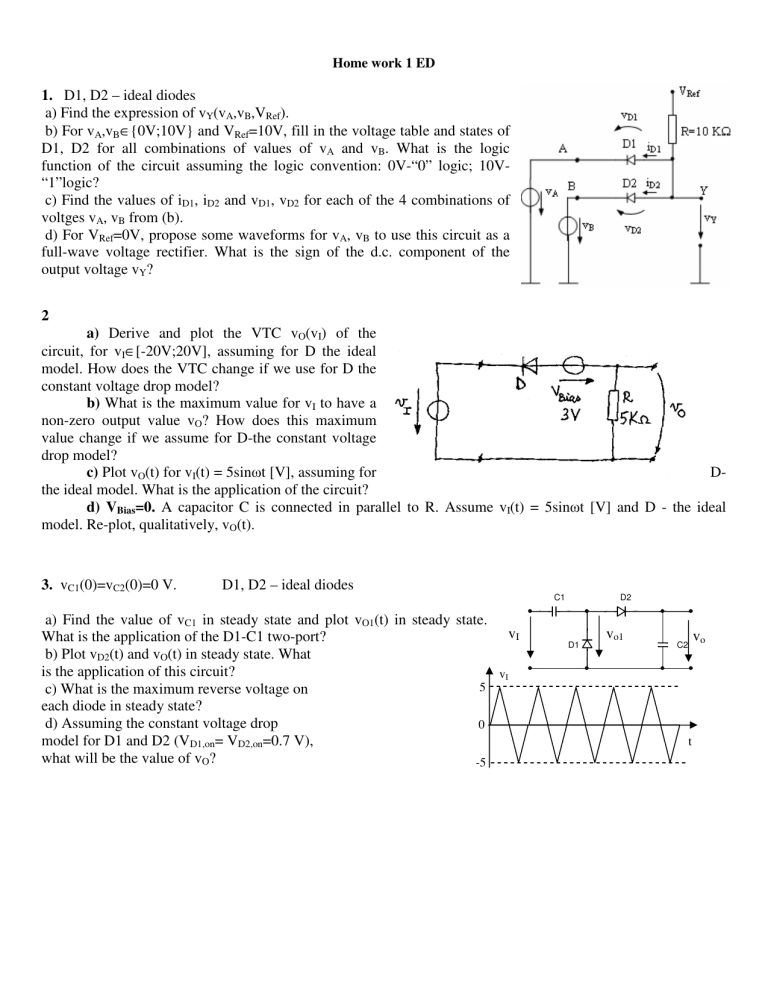
1. D1, D2 – ideal diodes
a) Find the expression of vY(vA,vB,VRef).
b) For vA,vB∈{0V;10V} and VRef=10V, fill in the voltage table and states of
D1, D2 for all combinations of values of vA and vB. What is the logic
function of the circuit assuming the logic convention: 0V-“0” logic; 10V“1”logic?
c) Find the values of iD1, iD2 and vD1, vD2 for each of the 4 combinations of
voltges vA, vB from (b).
d) For VRef=0V, propose some waveforms for vA, vB to use this circuit as a
full-wave voltage rectifier. What is the sign of the d.c. component of the
output voltage vY?
2
a) Derive and plot the VTC vO(vI) of the
circuit, for vI∈[-20V;20V], assuming for D the ideal
model. How does the VTC change if we use for D the
constant voltage drop model?
b) What is the maximum value for vI to have a
non-zero output value vO? How does this maximum
value change if we assume for D-the constant voltage
drop model?
c) Plot vO(t) for vI(t) = 5sinωt [V], assuming for
Dthe ideal model. What is the application of the circuit?
d) VBias=0. A capacitor C is connected in parallel to R. Assume vI(t) = 5sinωt [V] and D - the ideal
model. Re-plot, qualitatively, vO(t).
3. vC1(0)=vC2(0)=0 V.
D1, D2 – ideal diodes
C1
a) Find the value of vC1 in steady state and plot vO1(t) in steady state.
vI
What is the application of the D1-C1 two-port?
b) Plot vD2(t) and vO(t) in steady state. What
is the application of this circuit?
vI
5
c) What is the maximum reverse voltage on
each diode in steady state?
d) Assuming the constant voltage drop
0
model for D1 and D2 (VD1,on= VD2,on=0.7 V),
what will be the value of vO?
-5
D2
D1
vo1
vo
C2
t


