Simple Circuit Removes Sync or has
Negative Going Sync Tip
®
Technical Brief
July 20, 2006
TB462.1
Authors: Rudy Berneike and David Laing
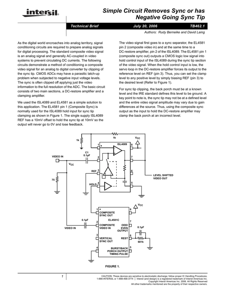
The video signal first goes to a sync separator, the EL4581
pin 2 (composite video in) and at the same time to a
DC-restore amplifier, pin 2 of the ISL4089. The EL4581 pin 1
(composite sync out) outputs a CMOS logic low signal into
hold control input of the ISL4089 during the sync tip section
of the video signal. When the hold control input is low, the
servo loop in the DC-restore amplifier forces its output to the
reference level on REF (pin 3). Thus, you can set the clamp
level to any positive level by simply biasing REF (pin 3) to
the desired level (Refer to Figure 1).
As the digital world encroaches into analog territory, signal
conditioning circuits are required to prepare analog signals
for digital processing. The standard composite video signal
is an analog signal and generally AC-coupled in video
systems to prevent circulating DC currents. The following
circuits demonstrate a method of conditioning a composite
video signal for an analog to digital converter by clipping of
the sync tip. CMOS ADCs may have a parasitic latch-up
problem when subjected to negative input voltage levels.
The sync is often clipped off applying just the video
information to the full resolution of the ADC. The basic circuit
consists of two main sections, a DC-restore amplifier and a
clamping amplifier.
For sync tip clipping, the back porch must be at a known
level and the IRE standard defines this level to be ground. A
key point to note is, the sync tip may not be at a defined level
and the entire video signal amplitude may vary due to gain
differences at the source. Thus, using the composite sync
output as the input to hold the DC-restore amplifier may
clamp the back porch at an incorrect level.
We used the ISL4089 and EL4581 as a simple solution to
this application. The EL4581 pin 1 (Composite Sync) is
normally used for the ISL4089 hold input for sync tip
clamping as shown in Figure 1. The single supply ISL4089
REF has a 10mV offset to hold the sync tip at 10mV so the
output will never go to 0V and lose feedback.
VCC
1k
1k
ISL4089
1
8
C1
0.1µF
VIDEO IN
+
7
2
VCC
REF 3
6
+
-
LEVEL SHIFTED
VIDEO OUT
75
HOLD
5
4
VCC
1
8
COMPOSITE
SYNC OUT
0.1µF
2
EL4581C
COMPOSITE
VIDEO IN
VIDEO IN
7
ODD/
EVEN
OUTPUT
3
6
VERTICAL
SYNC OUT
4
0.1µF
REST
681k
BURST/BACK 5
PORCH OUTPUT
TIMING PULSE
FIGURE 1.
1
CAUTION: These devices are sensitive to electrostatic discharge; follow proper IC Handling Procedures.
1-888-INTERSIL or 1-888-468-3774 | Intersil (and design) is a registered trademark of Intersil Americas Inc.
Copyright Intersil Americas Inc. 2006. All Rights Reserved
All other trademarks mentioned are the property of their respective owners.
Technical Brief 462
Low Cost Sync Clip
The ISL4089 can make use of the back porch output of the
EL4581C to generate the hold timing, but the ISL4089 can
have a slower recovery time than needed by some high end
applications. Also, the REF input has a 10mV fixed offset
which would place the back porch at 10mV above ground.
This 10mV offset will leave 10mV of sync tip on the output.
Below 100mV, the DC Restore linearity is somewhat
reduced. One method of improving the linearity at these low
levels is to simply DC couple the output load to ground,
which will also clamp the output to ground. Thus, the
ISL4089 makes a good low cost sync tip striper for removing
Sync On Green (SOG) used in both consumer games and
video products. Yet, a simple two-step solution will support
both consumer video and high performance video
requirements.
High Performance Sync Clip that
Removes Offsets
The EL4581 back porch output is used to set the sample and
hold window of the DC-restore amp. When the back porch
output goes low, the video signal will be clamped to a fixed
offset reference on REF (pin 3) of the ISL4089. The single
supply clipping amplifier with an offset will remove the sync
portion of the video signal.
By applying a positive offset voltage to REF input (pin 3) and
using back porch output of the EL4581, pin 5, to drive the
HOLD input (pin 4 of the EL4089), the back porch is now at
the proper voltage to prevent the sync tip from being clipped
at the output. EL4089 pin 4 going low, forces the necessary
offset voltage to be placed across the sample and hold
capacitor to create the proper input to output voltage shift. In
the design example, C1, the AC-coupling capacitor doubles
as a sample and hold capacitor. Photo 1 shows the analog
video input and the sync separator back porch output
waveforms.
Second, you will need to offset the sync stripper. Resistor
offsetting of the ISL4089 will have a residual offset resulting
in a 10mV sync tip. Yet, you can use an OpAmp to eliminate
the offset and thus eliminate the residual sync tip. We use
the EL8100 to remove both the 10mV offset and the addition
0.788V offset added at the input of the ISL4089.
More Details
First, adding the offset - A simple resistor voltage divider tied
to pin 3 of the ISL4089 will offset the input by the desired
0.8V. Tie a 4.22kΩ resistor from the +5V supply in series to
ground with an 806Ω resistor. Connect the junction to pin 3
of the ISL4089. This offsets the input by 0.8V and thus the
output will have the sync tip offset by +0.8V.
The ISL4089 as stated before, has a +10mV built-in offset on
REF (pin 3) allowing for single 5V operation and will need
additional offset adjustment to compensate for the +10mV
offset. The addition of a 43kΩ in parallel with the 806Ω will
compensate for the 10mV input offset. The final offset
applied to pin 3 will be 0.79V (0.800V- 0.01V). Note the
ISL4089 has an extra 1.2V offset built in to the pin 2 video
input for better linearity so if probed this will show an extra
1.2V offset. This does not effect the overall performance.
665
1k
1
C1
0.1µF
VIDEO IN
Vcc
8
+
2
7
REF 3
6
Vcc
4.22k
VIDEO OUT
+
75
806
-
43k
4
5
0.788V
OFFSET
FIGURE 2.
COMPOSITE
VIDEO INPUT
EL4581
BACK PORCH
SYNC OUTPUT
PHOTO 1. DC-RESTORE
Setting the Offset Voltage
First, you need to offset the REF input to the ISL4089, such
that the output back porch of the ISL4089 will be about 0.8V
above ground to retain sync tip.
2
Second, offset the sync stripper output - You need to
compensate for the output offset of the ISL4089 to set the
back porch at ground at the EL8100 output. Using the
feedback path, place an 806Ω resistor from EL8100 pin 6
(VOUT) to pin 1 negative input and add a second resistor
4.22kΩ from pin 8 (VCC) to pin 2. This will offset the sync
stripper output down by 0.8V. Thus, the EL8100 will return
the back porch to ground reference and strip off the sync tip.
The 4.22kΩ and 806Ω resistors should be 0.1% tolerance for
offset cancellation to be only 1.6mV error max or they can be
1% with a max error of 16mV. By using the same type
resistors for both offsetting networks, the ratio match of 1%
resistors will be about 4 to 5 times better than 1%, so the
error will typically be about 3mV to 4mV. The 43kΩ at 1%
gives an error of 0.1mV plus 0.5mV for 5% supply change.
TB462.1
July 20, 2006
Technical Brief 462
A gain of 1 is needed for some cases so the ISL4089 gain
can be set to 1 by removing the 1k gain resistor and
changing the feedback resistor to 0Ω. This will give an
overall gain of 1.2. If the gain must be 1, then use an output
divider on the EL8100 output of 200Ω series with 1kΩ to
ground and their junction is the output.
0.8V
OFFSET
806
VCC
VCC
1
4.22k
8
EL8100
DC-Restore with Back Porch at Ground
and Minus Sync Tip
7
2
-
VIDEO OUT
LEVEL
SHIFTED
VIDEO IN
3
+
6
75
75
5
4
This circuit may be converted to provide video output with
minus sync tip. Changing the clamp amp EL8100 to a dual
supply, ±5V amp, such as the EL5160, will keep the back
porch at ground with minus going sync tip (see Figure 4).
0.8V
OFFSET
806
VCC
FIGURE 3.
This feedback circuit also changes the gain of the EL8100 to
about AV = 1.2. The overall circuit gain of the ISL4089 and
ISL8100 must be a gain of 2 to recover from the double
termination losses.
The EL8100 has a gain of 1.2. Thus, the ISL4089 will need a
gain of 1.6 to give the overall circuit a gain of 2.0. The
feedback circuit, to have a gain of 1.6, computes to be 625Ω
in the feedback loop and 1kΩ to ground. The closest
standard 1% resistor is 665Ω.
The EL8100 stage limits the negative excursion to the
ground level. The input range of the EL8100 is 0V to 3.5V
and output is 0V to 5V. Its fast 7ns of negative over-drive
recovery makes it ideal for clamping applications (see
Figure 5).
1
4.22k
+VCC
8
EL5160
2
7
-
LEVEL
SHIFTED
VIDEO IN
3
4
+
VIDEO OUT
6
5
75
75
-VSS
FIGURE 4. DC-RESTORE WITH NEGATIVE SYNC TIP OUTPUT
Photo 2 shows the incoming video signal whose back porch
is clamped to the ground level and the amplifier output signal
with negative going portion of the sync tip clipped off.
“CLAMPED”
COMPOSITE
VIDEO INPUT
“SYNC-LESS”
VIDEO OUTPUT
PHOTO 2. “SYNC-LESS” VIDEO SIGNAL
3
TB462.1
July 20, 2006
Technical Brief 462
The Final Design:
0.8V
OFFSET
1
ISL4089
8
1
C1
0.1µF
VIDEO IN
806
VCC
665
1k
4.22k
+
2
7
3
6
8
EL8100
2
VCC
7
-
4.22k
+
75
VCC
43k
4
806
VIDEO OUT
3
-
5
+
4
6
5
75
75
0.788V
OFFSET
VCC
1
8
VCC = 5.0V
7
RESISTORS:
STANDARD VALUES
METAL FILM
±1%
COMPOSITE
SYNC OUT
0.1µF
2
EL4581C
COMPOSITE
VIDEO IN
ODD/
EVEN
OUTPUT
3
0.1µF
6
VERTICAL
SYNC OUT
REST
4
681k
5
BURST/BACK
PORCH OUTPUT
FIGURE 5.
Intersil Corporation reserves the right to make changes in circuit design, software and/or specifications at any time without notice. Accordingly, the reader is cautioned to
verify that the Application Note or Technical Brief is current before proceeding.
For information regarding Intersil Corporation and its products, see www.intersil.com
4
TB462.1
July 20, 2006
