Solid State Phenomena Vols. 121-123 (2007) pp 693-696
Online available since 2007/Mar/15 at www.scientific.net
© (2007) Trans Tech Publications, Switzerland
doi:10.4028/www.scientific.net/SSP.121-123.693
High-frequency capability of Schottky-barrier carbon nanotube FETs
L.C. Castroa, D.L. Pulfreyb and D.L. Johnc
Department of Electrical Engineering, University of British Columbia,
2356 Main Mall, Vancouver, BC, V6T 1Z4, Canada
a
b
c
leonardo@ece.ubc.ca, pulfrey@ece.ubc.ca, davej@ece.ubc.ca
Keywords: carbon nanotube field-effect transistor, small-signal properties, high-frequency figures
of merit, resonance.
Abstract. The high-frequency capability of carbon nanotube field-effect transistors is investigated by
simulating the small-signal performance of a device with negative-barrier Schottky contacts for the
source and drain, and with a small, ungated region of nanotube between the end contacts and the edge
of the wrap-around gate electrode. The overall structure is shown to exhibit resonant behaviour,
which leads to a significant bias dependence of the small-signal capacitances and transconductance.
This could lead to high-frequency figures of merit (fT and fmax) in the terahertz regime.
Introduction
Carbon nanotube field-effect transistors (CNFETs) are predicted to have superior DC characteristics
to those of foreseeable silicon MOSFETs [1,2]. Experimentally, impressive values for drain current
and transconductance have already been reported in prototype devices [3]. However, the AC
performance of CNFETs has not yet received much attention [4], and the likelihood of
high-frequency operation needs to be established. Here, we take a step in this direction by predicting
two useful figures of merit for high-frequency transistors, namely: the unity current-gain and unity
power-gain frequencies, fT and fmax, respectively.
We employ the standard small-signal method [5], abetted by a self-consistent Schrödinger-Poisson
solver [6], in order to obtain preliminary estimates of these valuable figures of merit. In particular, we
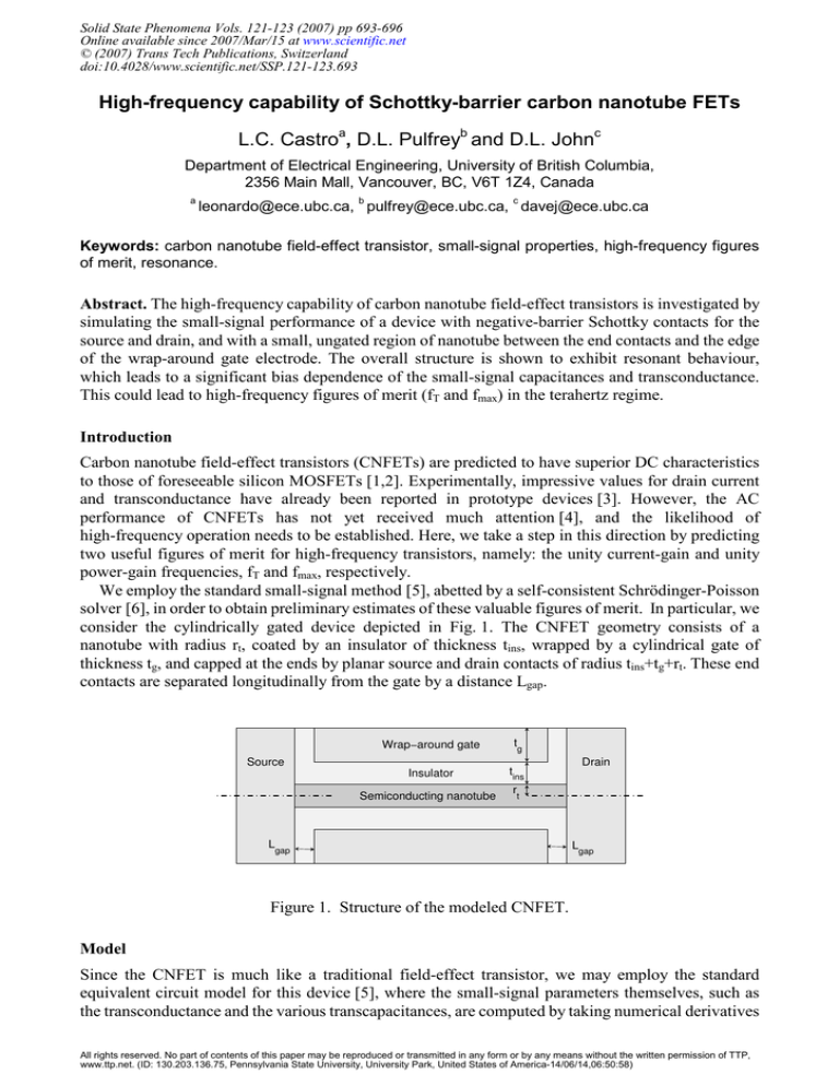
consider the cylindrically gated device depicted in Fig. 1. The CNFET geometry consists of a
nanotube with radius rt, coated by an insulator of thickness tins, wrapped by a cylindrical gate of
thickness tg, and capped at the ends by planar source and drain contacts of radius tins+tg+rt. These end
contacts are separated longitudinally from the gate by a distance Lgap.
Wrap−around gate
tg
Insulator
tins
Source
Semiconducting nanotube
Drain
r
t
L
gap
Lgap
Figure 1. Structure of the modeled CNFET.
Model
Since the CNFET is much like a traditional field-effect transistor, we may employ the standard
equivalent circuit model for this device [5], where the small-signal parameters themselves, such as
the transconductance and the various transcapacitances, are computed by taking numerical derivatives
All rights reserved. No part of contents of this paper may be reproduced or transmitted in any form or by any means without the written permission of TTP,
www.ttp.net. (ID: 130.203.136.75, Pennsylvania State University, University Park, United States of America-14/06/14,06:50:58)
694
Nanoscience and Technology
based on the results of self-consistent DC charge-voltage calculations [6,7]. Through our use of a
Schrödinger-Poisson solver for these DC results, we are able to include the effects of geometry,
quantum capacitance, and spatial non-uniformity of the charge in our calculations.
While we have previously presented results for the intrinsic fT with only three circuit elements [7],
here we consider the additional effects of series resistances associated with each of the terminals, and
we include the remaining capacitance components. This allows us to compute the extrinsic fT, and
also to consider fmax. For clarity, we include the standard equivalent circuit in Fig. 2, where we note
that the subscripts s, d and g refer to the source, drain and gate, respectively. In the usual way, we
consider the fT and fmax expressions, which may be arrived at by extrapolating the characteristic decay
in gain, from its value at an appropriate low frequency, to the 0dB point.
G
Rg
g
Cgs
S
Rs
gmvgs
s
Cgd
D
d
gds
Rd
Csd
Cmvgs
Figure 2. Small signal equivalent circuit. The transcapacitance Cm = Cdg - Cgd.
Results and Discussion
The model device in this study employs a (16,0) nanotube of radius 0.63nm, length 30nm, bandgap
0.62eV, unity relative permittivity, and effective mass 0.06m0, where m0 is the free electron rest mass.
Moreover, tins is 2.5nm, tg is 3nm, the insulator permittivity is 25 as is appropriate for zirconia [8], and
Lgap is 5nm for this initial investigation. The work function of the nanotube is taken to be 4.5eV, while
that of the end-contacts is 3.9eV, yielding negative-Schottky barrier, n-type transistor operation. All
results are for a drain-source voltage of 0.5V.
Fig. 3 illustrates the intrinsic parameters for our device. The oscillatory peaks in the capacitances
and transconductance are related to the formation of quasi-bound states in the short channel [7,9].
With the modulation of the applied voltage, the states, indicated by the bright patches in Fig. 4, are
shifted in energy by band bending in the channel. As they cross the source or drain Fermi level, they
become populated, and we obtain peaks in the charge accumulation and, consequently, in the
capacitances. Since the charge accumulation affects the amount of band bending in the channel
through our self-consistent DC calculations, we also see peaks in the transconductance gm. The gm
behaviour is complicated due to its dependence both on the charge and on the Fermi distributions at
the injecting contacts.
In Fig. 5, we present our main results, the predictions of fT and fmax for our model CNFET. Fig. 5(a)
shows fT for Rs = Rd set to 1kΩ, 10kΩ, and 100kΩ, and we recall that Rg has no influence on this
figure of merit. Note that the values of the parasitic resistors Rs and Rd are chosen to be comparable to
the contact resistance that results from mode constriction when carriers pass from a many-moded
Solid State Phenomena Vols. 121-123
695
material to a material with only a few modes [10]. In the carbon nanotube case, we consider the lowest
two degenerate modes in energy for an equivalent contact resistance of around 6-7kΩ. Note that the
contact resistance is automatically included in our self-consistent DC calculations, so an explicit
resistor is not needed to represent it in the equivalent circuit.. Thus, the resistors shown in Fig. 2 are
solely parasitic. It is evident that the maximum value of fT occurs at the first peak in gm. Turning now
to fmax, shown in Fig. 5(b), we focus on the effect of Rg, and show results for Rg set to 100Ω, 1kΩ, and
10kΩ, with Rs = Rd = 10kΩ. Again, a pronounced peak coincides with the first peak in gm.
0.4
Transconductance (4q /h)
Cgs
20
C
Capacitance (aF)
2
gd
C
15
sd
Cm
10
5
0
0
0.2
0.4
0.6
0.8
Gate voltage (V)
1
0.3
0.2
0.1
0
0
0.2
0.4
0.6
0.8
Gate voltage (V)
1
Figure 3. Capacitances and transconductance for the model device.
0.02
Energy (eV)
0
−0.02
−0.04
−0.06
−0.08
−0.1
0
5
10
15
z (nm)
20
25
30
Figure 4. Charge density for the model device subject to a gate-source voltage of 0.38V. Brighter
patches indicate higher charge density, while a portion of the conduction band edge is shown by the
white line. The energy values are referenced to the source Fermi level.
696
Nanoscience and Technology
1 kOhm
10 kOhm
100 kOhm
(a)
(GHz)
600
800
max
400
100 Ohm
1 kOhm
10 kOhm
(b)
600
400
f
T
f (GHz)
800
200
0
0
200
0.2
0.4
0.6
0.8
Gate voltage (V)
1
0
0
0.2
0.4
0.6
0.8
Gate voltage (V)
1
Figure 5. Extrapolated figures of merit: (a) fT with Rs = Rd set to 1kΩ (solid),
10kΩ (dashed), and 100kΩ (dotted), and (b) fmax with Rs = Rd = 10kΩ for Rg set
to 100Ω (solid), 1kΩ (dashed), and 10kΩ (dotted).
Conclusions
From this simulation of the high-frequency performance of CNFETs, it can be concluded that, in
short-channel devices, with negative-barrier Schottky contacts for the source and drain, and with very
short ungated regions, and where coherent transport is possible, resonance effects can lead to a strong
bias dependence of the high-frequency figures of merit, fT and fmax. At the resonance peaks, these
frequencies may reach the THz level.
References
[1] L.C. Castro, D.L. John and D.L. Pulfrey: Smart Mater. Struct. Accepted Aug. 13, 2004. [Online.]
Available: http://nano.ece.ubc.ca/pub/publications.htm.
[2] J. Guo, M. Lundstrom and S. Datta: Appl. Phys. Lett. Vol. 80 (2002), p. 3192.
[3] A. Javey, J. Guo, Q. Wang, M. Lundstrom and H. Dai: Nature Vol. 424 (2003), p. 654.
[4] D.V. Singh, K.A. Jenkins, J. Appenzeller, D. Neumayer, A. Gill and H.-S.P. Wong: IEEE Trans.
Nanotechnol. Vol. 3 (2004), p. 383.
[5] Y.P. Tsividis: Operation and Modeling of the MOS Transistor, Chapter 9, (McGraw-Hill,
Toronto 1987).
[6] D.L. John, L.C. Castro, P.J.S. Pereira and D.L. Pulfrey: Proc. NSTI Nanotech Vol. 3 (2004),
p. 65.
[7] L.C. Castro, D.L. John, D.L. Pulfrey, M. Pourfath, A. Gehring and H. Kosina: IEEE Trans.
Nanotechnol. Submitted Nov. 16, 2004.
[8] A. Javey, R. Tu, D. Farmer, J. Guo, R. Gordon and H. Dai: Nano Lett. Vol. 5 (2005), p. 345.
[9] D.L. John, L.C. Castro and D.L. Pulfrey: J. Appl. Phys. Vol. 96 (2004), p. 5180.
[10] S. Datta: Electronic Transport in Mesoscopic Systems (Cambridge University Press, New York
1995).
Nanoscience and Technology
10.4028/www.scientific.net/SSP.121-123
High-Frequency Capability of Schottky-Barrier Carbon Nanotube FETs
10.4028/www.scientific.net/SSP.121-123.693
DOI References
[2] J. Guo, M. Lundstrom and S. Datta: Appl. Phys. Lett. Vol. 80 (2002), p. 3192.
doi:10.1063/1.1469208
[5] Y.P. Tsividis: Operation and Modeling of the MOS Transistor, Chapter 9, (McGraw-Hill, oronto 1987).
doi:10.1109/JSSC.1987.1052727
[8] A. Javey, R. Tu, D. Farmer, J. Guo, R. Gordon and H. Dai: Nano Lett. Vol. 5 (2005), p. 345.
doi:10.1021/nl047931j
[5] Y.P. Tsividis: Operation and Modeling of the MOS Transistor, Chapter 9, (McGraw-Hill, Toronto 1987).
doi:10.1109/JSSC.1987.1052727
