UM2053
User manual
14 mm x 14 mm antenna reference board
for the M24SR64-Y dual interface EEPROM
Introduction
The ANT7-T-M24SR64 is a ready-to-use demonstration board intended to evaluate the
M24SR64-Y dual interface Electrically Erasable Programmable Memory (EEPROM), a
device featuring an I2C interface that can be operated from an external power supply. The
M24SR64-Y is a contactless memory, powered by the received carrier electromagnetic field.
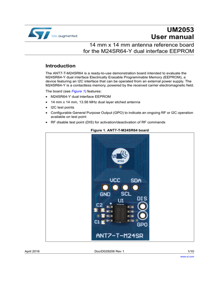
The board (see Figure 1) features:
• M24SR64-Y dual interface EEPROM
• 14 mm x 14 mm, 13.56 MHz dual layer etched antenna
• I2C test points
• Configurable General Purpose Output (GPO) to indicate an ongoing RF or I2C operation
available on test point
• RF disable test point (DIS) for activation/deactivation of RF commands
Figure 1. ANT7-T-M24SR64 board
April 2016
DocID029206 Rev 1
1/10
www.st.com
1
Contents
UM2053
Contents
1
2
Hardware description . . . . . . . . . . . . . . . . . . . . . . . . . . . . . . . . . . . . . . . . 5
1.1
Startup . . . . . . . . . . . . . . . . . . . . . . . . . . . . . . . . . . . . . . . . . . . . . . . . . . . . 5
1.2
Using RF disable (DIS) pin . . . . . . . . . . . . . . . . . . . . . . . . . . . . . . . . . . . . . 6
1.3
Using General Purpose Output (GPO) pin . . . . . . . . . . . . . . . . . . . . . . . . . 6
1.4
Using I2C pins . . . . . . . . . . . . . . . . . . . . . . . . . . . . . . . . . . . . . . . . . . . . . . 6
Component description . . . . . . . . . . . . . . . . . . . . . . . . . . . . . . . . . . . . . . 7
2.1
M24SR64-Y . . . . . . . . . . . . . . . . . . . . . . . . . . . . . . . . . . . . . . . . . . . . . . . . 7
3
Schematics . . . . . . . . . . . . . . . . . . . . . . . . . . . . . . . . . . . . . . . . . . . . . . . . 7
4
Federal Communications Commission (FCC) and
Industry Canada (IC) compliance statements . . . . . . . . . . . . . . . . . . . . . 8
4.1
4.2
5
2/10
FCC Compliance Statement . . . . . . . . . . . . . . . . . . . . . . . . . . . . . . . . . . . . 8
4.1.1
Part 15.19 . . . . . . . . . . . . . . . . . . . . . . . . . . . . . . . . . . . . . . . . . . . . . . . . 8
4.1.2
Part 15.105 . . . . . . . . . . . . . . . . . . . . . . . . . . . . . . . . . . . . . . . . . . . . . . . 8
4.1.3
Part 15.21 . . . . . . . . . . . . . . . . . . . . . . . . . . . . . . . . . . . . . . . . . . . . . . . . 8
Formal notices required by the Industry Canada (“IC”) . . . . . . . . . . . . . . . 8
4.2.1
Compliance Statement . . . . . . . . . . . . . . . . . . . . . . . . . . . . . . . . . . . . . . . 8
4.2.2
Declaration de Conformité . . . . . . . . . . . . . . . . . . . . . . . . . . . . . . . . . . . . 8
Revision history . . . . . . . . . . . . . . . . . . . . . . . . . . . . . . . . . . . . . . . . . . . . 9
DocID029206 Rev 1
UM2053
List of tables
List of tables
Table 1.
Table 2.
M24SR64-Y . . . . . . . . . . . . . . . . . . . . . . . . . . . . . . . . . . . . . . . . . . . . . . . . . . . . . . . . . . . . . 7
Document revision history . . . . . . . . . . . . . . . . . . . . . . . . . . . . . . . . . . . . . . . . . . . . . . . . . . 9
DocID029206 Rev 1
3/10
3
List of figures
UM2053
List of figures
Figure 1.
Figure 2.
Figure 3.
4/10
ANT7-T-M24SR64 board . . . . . . . . . . . . . . . . . . . . . . . . . . . . . . . . . . . . . . . . . . . . . . . . . . . 1
Functional block diagram . . . . . . . . . . . . . . . . . . . . . . . . . . . . . . . . . . . . . . . . . . . . . . . . . . . 5
ANT7-T-M24SR64 hardware schematics . . . . . . . . . . . . . . . . . . . . . . . . . . . . . . . . . . . . . . . 7
DocID029206 Rev 1
UM2053
1
Hardware description
Hardware description
The ANT7-T-M24SR64 (see Figure 2) contains the M24SR64-Y EEPROM device and a
14 mm x 14 mm, 13.56 MHz dual layer etched antenna.
Figure 2. Functional block diagram
9&&
PP;PP
$QWHQQDORRS
',6
*32
065<
6'$
*1'
6&/
069
The M24SR64-Y is a dynamic NFC Forum Type 4 Tag – ISO/IEC 14443 with 25 pF internal
tuning capacitance. Memory size is 64 Kbits with NDEF support, that can be accessed
either by I2C interface or by 13.56 MHz air interface.
The tag features a user configurable digital output pin toggling during either RF or I2C
operation.
The M24SR64-Y also provides an input used to disable the RF communication.
As shown in Figure 1, all M24SR64-Y pins (except AC0 and AC1, related to antenna
connection) are made available to the user, with 1.2 mm diameter through-hole test points.
1.1
Startup
The ANT7-T-M24SR64 is already programmed with an URI that will automatically redirect to
the associated ST web-page.
User has to:
•
Enable NFC on the phone (Settings → Wireless and Networks → NFC) and make sure
it is also connected to the Internet
•
Bring the phone close to the ANT7-T-M24SR64 antenna to be redirected to the ST25
web-page.
Various usages of the ANT7-T-M24SR64 with a smartphone are allowed with ST25 NFC
Demo application for Android.
To download the application and for more use cases details user should visit the dedicated
pages on https://play.google.com and on www.st.com.
It is also possible to access the M24SR64-Y memory with CR95HF demonstration board
and associated PC software available on www.st.com.
DocID029206 Rev 1
5/10
9
Hardware description
1.2
UM2053
Using RF disable (DIS) pin
This active high signal is used to disable the RF communication.
When the voltage on the VCC pin is below the POR level or not connected, an internal
pull-down resistor is connected on this pad. Thus, the RF disable pad is maintained to the
low level and the RF analog front end is activated. When the voltage on the VCC pin is
higher than the POR level, the I2C host shall set this pin to disable the RF communication.
In Dual interface mode, the DIS pin must not be left floating.
1.3
Using General Purpose Output (GPO) pin
This configurable output signal is used either to indicate that the M24SR64-Y is executing
an I2C or RF session in the mode chosen by the user. It is an open drain output and a
pull-up resistor (20 kΩ) must be connected between GPO and VCC pins. This digital output
pin is easily accessible to the user on the GPO test point.
1.4
Using I2C pins
The memory is accessible through I2C when it is powered by the VCC pin. I2C clock and
data signals are respectively available on SCL and SDA test points. Since I2C is an open
drain interface, pull up resistors have to be connected from both lines to VCC pin.
6/10
DocID029206 Rev 1
UM2053
Component description
2
Component description
2.1
M24SR64-Y
The M24SR64-Y device is a Dynamic NFC/RFID tag IC with a dual interface, electrically
erasable programmable memory (EEPROM). It features an I2C interface and can be
operated from a VCC power supply. It is also a contactless memory powered by the received
carrier electromagnetic field.
Table 1. M24SR64-Y
Description
Sales type
M24SR64-YMN6
Package
SO8N
Operating voltage
2.7 to 5.5 Volts
Schematics
Figure 3. ANT7-T-M24SR64 hardware schematics
Antenne
i
VCC
U1
M24SR64-YMN6T/2
SCL
3
SDA
4
22-29-2041-NC
1.2mm
RF_DIS
GPO
1
7
6
5
RF DIS
GPO
VCC
GPO
2
AC0
SCL
SDA
AC1
C2
NC
GND
2
ANTENNA
3
VSS
1.2mm
1
8
RFDIS
J1
4
3
Feature
C1
NC
GND
GND
DocID029206 Rev 1
GND
7/10
9
Federal Communications Commission (FCC) and Industry Canada (IC) compliance statements
4
Federal Communications Commission (FCC) and
Industry Canada (IC) compliance statements
4.1
FCC Compliance Statement
4.1.1
Part 15.19
This device complies with Part 15 of the FCC Rules. Operation is subject to the following
two conditions: (1) this device may not cause harmful interference, and (2) this device must
accept any interference received, including interference that may cause undesired
operation.
4.1.2
Part 15.105
This equipment has been tested and found to comply with the limits for a Class A digital
device, pursuant to part 15 of the FCC Rules. These limits are designed to provide
reasonable protection against harmful interference when the equipment is operated in a
commercial environment. This equipment generates, uses, and can radiate radio frequency
energy and, if not installed and used in accordance with the instruction manual, may cause
harmful interference to radio communications. Operation of this equipment in a residential
area is likely to cause harmful interference in which case the user will be required to correct
the interference at his own expense.
4.1.3
Part 15.21
Any changes or modifications to this equipment not expressly approved by
STMicroelectronics may cause harmful interference and void the user’s authority to operate
this equipment
4.2
Formal notices required by the Industry Canada (“IC”)
4.2.1
Compliance Statement
This device complies with Industry Canada licence-exempt RSS standard(s). Operation is
subject to the following two conditions : (1) this device may not cause interference, and (2)
this device must accept any interference, including interference that may cause undesired
operation.
4.2.2
Declaration de Conformité
Le présent appareil est conforme aux CNR d’Industrie Canada applicables aux appareils
radio exempts de licence. L’exploitation est autorisée aux deux conditions suivantes : (1)
l’appareil ne doit pas produire de brouillage, et (2) l’utilisateur de l’appareil doit accepter tout
brouillage radioélectrique subi, même si le brouillage est susceptible d’en compromettre le
fonctionnement.
8/10
DocID029206 Rev 1
UM2053
5
Revision history
Revision history
Table 2. Document revision history
Date
Revision
21-Apr-2016
1
Changes
Initial release.
DocID029206 Rev 1
9/10
9
UM2053
IMPORTANT NOTICE – PLEASE READ CAREFULLY
STMicroelectronics NV and its subsidiaries (“ST”) reserve the right to make changes, corrections, enhancements, modifications, and
improvements to ST products and/or to this document at any time without notice. Purchasers should obtain the latest relevant information on
ST products before placing orders. ST products are sold pursuant to ST’s terms and conditions of sale in place at the time of order
acknowledgement.
Purchasers are solely responsible for the choice, selection, and use of ST products and ST assumes no liability for application assistance or
the design of Purchasers’ products.
No license, express or implied, to any intellectual property right is granted by ST herein.
Resale of ST products with provisions different from the information set forth herein shall void any warranty granted by ST for such product.
ST and the ST logo are trademarks of ST. All other product or service names are the property of their respective owners.
Information in this document supersedes and replaces information previously supplied in any prior versions of this document.
© 2016 STMicroelectronics – All rights reserved
10/10
DocID029206 Rev 1

