OTAs-based Positive/Negative Floating Inductance Simulator
advertisement
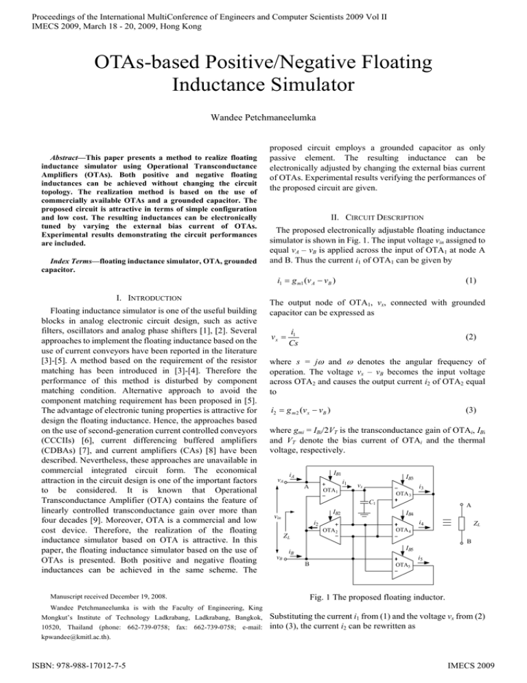
Proceedings of the International MultiConference of Engineers and Computer Scientists 2009 Vol II IMECS 2009, March 18 - 20, 2009, Hong Kong OTAs-based Positive/Negative Floating Inductance Simulator Wandee Petchmaneelumka Abstract—This paper presents a method to realize floating inductance simulator using Operational Transconductance Amplifiers (OTAs). Both positive and negative floating inductances can be achieved without changing the circuit topology. The realization method is based on the use of commercially available OTAs and a grounded capacitor. The proposed circuit is attractive in terms of simple configuration and low cost. The resulting inductances can be electronically tuned by varying the external bias current of OTAs. Experimental results demonstrating the circuit performances are included. Index Terms—floating inductance simulator, OTA, grounded capacitor. proposed circuit employs a grounded capacitor as only passive element. The resulting inductance can be electronically adjusted by changing the external bias current of OTAs. Experimental results verifying the performances of the proposed circuit are given. II. CIRCUIT DESCRIPTION The proposed electronically adjustable floating inductance simulator is shown in Fig. 1. The input voltage vin assigned to equal vA – vB is applied across the input of OTA1 at node A and B. Thus the current i1 of OTA1 can be given by i1 = g m1 (v A − v B ) I. INTRODUCTION Floating inductance simulator is one of the useful building blocks in analog electronic circuit design, such as active filters, oscillators and analog phase shifters [1], [2]. Several approaches to implement the floating inductance based on the use of current conveyors have been reported in the literature [3]-[5]. A method based on the requirement of the resistor matching has been introduced in [3]-[4]. Therefore the performance of this method is disturbed by component matching condition. Alternative approach to avoid the component matching requirement has been proposed in [5]. The advantage of electronic tuning properties is attractive for design the floating inductance. Hence, the approaches based on the use of second-generation current controlled conveyors (CCCIIs) [6], current differencing buffered amplifiers (CDBAs) [7], and current amplifiers (CAs) [8] have been described. Nevertheless, these approaches are unavailable in commercial integrated circuit form. The economical attraction in the circuit design is one of the important factors to be considered. It is known that Operational Transconductance Amplifier (OTA) contains the feature of linearly controlled transconductance gain over more than four decades [9]. Moreover, OTA is a commercial and low cost device. Therefore, the realization of the floating inductance simulator based on OTA is attractive. In this paper, the floating inductance simulator based on the use of OTAs is presented. Both positive and negative floating inductances can be achieved in the same scheme. The Manuscript received December 19, 2008. (1) The output node of OTA1, vx, connected with grounded capacitor can be expressed as vx = i1 Cs (2) where s = jω and ω denotes the angular frequency of operation. The voltage vx – vB becomes the input voltage across OTA2 and causes the output current i2 of OTA2 equal to i2 = g m 2 (v x − v B ) (3) where gmi = IBi/2VT is the transconductance gain of OTAi, IBi and VT denote the bias current of OTAi and the thermal voltage, respectively. vA IB1 iA i1 A OTA1 IB3 vx i3 OTA 3 C1 IB2 vin A IB4 i4 i2 OTA2 ZL vB ZL OTA 4 B IB5 iB i5 B OTA5 Fig. 1 The proposed floating inductor. Wandee Petchmaneelumka is with the Faculty of Engineering, King Mongkut’s Institute of Technology Ladkrabang, Ladkrabang, Bangkok, 10520, Thailand (phone: 662-739-0758; fax: 662-739-0758; e-mail: Substituting the current i1 from (1) and the voltage vx from (2) into (3), the current i2 can be rewritten as kpwandee@kmitl.ac.th). ISBN: 978-988-17012-7-5 IMECS 2009 Proceedings of the International MultiConference of Engineers and Computer Scientists 2009 Vol II IMECS 2009, March 18 - 20, 2009, Hong Kong i2 = g m1 g m 2 (v A − v B ) − g m 2 v B Cs (4) If (gm1gm2/Cω) >> gm2 is chosen, then the current i2 can be approximated as i2 = g m1 g m 2 (v A − v B ) Cs (5) Also, the voltage vx – vB is used as the input voltage across the OTA3, OTA4, and OTA5. Therefore the relation between the output currents i3, i4, and i5 of OTA3, OTA4, and OTA5, respectively, and the current i2 can be given by i3 = − i4 = g m3 I i2 = − B 3 i2 g m2 I B2 g m4 I i2 = B 4 i2 g m2 I B2 i5 = − g m5 I i2 = − B 5 i2 g m2 I B2 (6) (7) Leq = 4VT2C I B1 I B 2 (1 − K ) (17) From (17), it clearly seems that proposed floating inductance can be obtained in the same circuit by adjusting either the bias current ratio K or the current IB1. Moreover, the positive inductance can be achieved for K < 1. Otherwise, the resulting inductance will be negative for K > 1. III. EXPERIMENTAL RESULTS To demonstrate the performances of the proposed inductance simulator, the floating inductor as shown in Fig. 1 was experimentally implemented using the commercially available OTA CA3280 devices. The grounded capacitor C1 of the proposed inductor in Fig. 1 was set to 100nF. The bias currents IB2 = IB3 and IB4 = IB5 were varied to achieve the current gain variation. (8) The bias currents IB2 and IB4 are assigned to equal IB3 and IB5, respectively. The currents i3, i4, and i5 can be rewritten as i3 = −i2 (9) i4 = Ki2 (10) i5 = − Ki2 (11) where K = IB4/IB2 = IB5/IB2 is the bias current ratio. The currents iA and iB at node A and B, respectively, can be obtained as i A = −i3 − i4 (12) iB = −i2 − i5 (13) (a) Substituting the currents i3 and i4 from (9) and (10), respectively, into (12) and i5 from (11) into (13), the current iA and iB can be state as i A = i2 − Ki2 = (1 − K )i2 (14) iB = −i2 + Ki2 = −(1 − K )i2 (15) It can be seen that the currents iA and iB are equal in magnitude, but opposite in their flowing directions. Considering the voltages vA and vB across node A and B and the current directions iA and iB, the obtained impedance of proposed inductance simulator ZL can be state as ZL = v A − vB Cs 4VT2Cs = = iA g m1 g m 2 (1 − K ) I B1 I B 2 (1 − K ) (b) (16) Thus the value of the resulting inductance Leq from circuit in Fig. 1 can be given by ISBN: 978-988-17012-7-5 Fig. 2 The plots of the measured floating inductances against the varied bias current IB1. (a) positive inductance (b) negative inductance IMECS 2009 Proceedings of the International MultiConference of Engineers and Computer Scientists 2009 Vol II IMECS 2009, March 18 - 20, 2009, Hong Kong Figs. 2(a) ~ 2(b) show the plots of the measured values of the positive and negative floating inductances Leq, respectively, against the bias current IB1 varied from 10μA to 1.5mA. The bias current gain K = 0.82 and K = 1.5 are chosen to achieve the positive value in Fig. 2(a) and negative value in Fig. 2(b), respectively. It is evident that both positive and negative inductances can be achieved in the same scheme by adjusting the external bias current of OTAs. The proposed positive and negative floating inductors employed in voltage amplifier is shown in Fig. 3, where R = 1kΩ is the constant resistor. Figs. 4(a) ~ 4(b) demonstrate the measured results of the voltage amplifier for positive and negative inductances, where 20 kHz sinusoidal input voltage vi of peak amplitude 50mV was applied and Leq = 7.98mH and Leq = -7.98mH were chosen to obtain the output voltage vo = 2vi and vo = -2vi, respectively. R Leq vi Op amp vo Fig. 5 The proposed positive floating inductor in RLC low-pass filter. vo(t) / vi (t) Fig. 3 The proposed positive and negative floating inductances in voltage amplifier. Fig. 6 Frequency responses of the low-pass filter. (a) The proposed floating inductor is applied in RLC low-pass filter as shown in Fig. 5. From Fig. 5, the resistor R and the capacitor CL were set to 33Ω and 0.22μF, respectively. The proposed floating inductances Leq = 5mH, 1mH and 500μH were chosen to achieved the resonance frequencies of the low-pass filter at 5kHz, 10kHz and 15kHz, respectively. Fig. 6 shows plots of the frequency responses of the low- pass filter in Fig. 5. It should be noted that both proposed positive and negative floating inductance simulators can be employed in analog electronic circuit design. IV. CONCLUSION (b) Fig. 4 The measured results of the voltage amplifier. (a) for positive inductance (b) for negative inductance ISBN: 978-988-17012-7-5 The electronically adjustable floating inductance simulator has been described in this paper. The proposed inductance simulator is based on the use of OTAs and a grounded capacitor. Both positive and negative inductances are obtained in the same circuit. The magnitude of the resulting inductance can be electronically varied by changing the external bias current of OTAs. Experimental results verifying the basic performances of the proposed floating inductor are agreed with the expected values. IMECS 2009 Proceedings of the International MultiConference of Engineers and Computer Scientists 2009 Vol II IMECS 2009, March 18 - 20, 2009, Hong Kong REFERENCES [1] [2] [3] [4] [5] [6] [7] [8] [9] J. Malhota and R. Senani, “Class of floating, generalized positive/negative immittance converters/inverters realized with operational mirrored amplifiers,” Electron. Lett., vol. 30, no. 1, 1994, pp. 3-5. A. Thanachayanont and A. Payne, “CMOS floating active inductor and its application to bandpass filter and oscillator designs, ” IEE Proc. Circuits Device Syst., vol. 147, 2000, pp. 42-48. K. Pal, “Novel floating inductance using current conveyors,” Electron. Lett., vol. 17, no. 18, 1981, pp. 638. V. Singh, “Active RC single-resistance-controlled lossless floating inductance simulation using single grounded capacitor,” Electron. Lett., vol. 17, no. 24, 1981, pp. 920-921. R. Senani, “Novel lossless synthetic floating inductor employing a grounded capacitor,” Electron. Lett., vol. 18, no. 10, 1982, pp. 413-414. W. Kiranon and P. Pawarangkoon, “Floating inductance simulation based on current conveyors,” Electron. Lett., vol. 33, no. 21, 1997, pp. 1748-1749. A. U. Keskin and E. Hangcioglu, “CDBA-based synthetic floating inductance circuits with electronic tuning properties,” ETRI J., vol. 27, no. 2, 2005, pp. 239-242. P. Costas and S. Asimina, “Curent amplifier based grounded and floating inductance simulators,” Int. J. Electron. Commun. (AEU), vol. 60, 2006, pp. 168-171. S. Soclof, Design and applications of analog integrated circuit, Singapore: Prentice Hall Inc., 1997, pp. 464-473. ISBN: 978-988-17012-7-5 IMECS 2009
