APW34063 - Anpec Electronics
advertisement

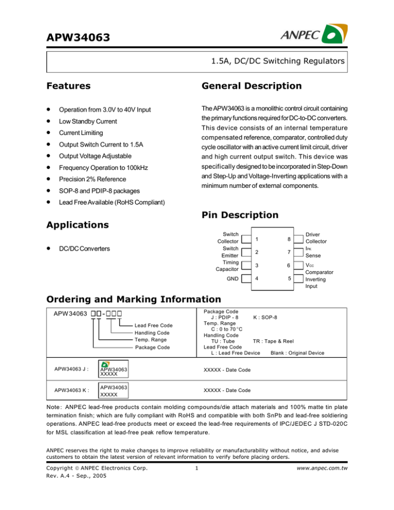
APW34063 1.5A, DC/DC Switching Regulators Features General Description • • • • • • • • • The APW34063 is a monolithic control circuit containing the primary functions required for DC-to-DC converters. This device consists of an internal temperature compensated reference, comparator, controlled duty cycle oscillator with an active current limit circuit, driver and high current output switch. This device was specifically designed to be incorporated in Step-Down and Step-Up and Voltage-Inverting applications with a minimum number of external components. Operation from 3.0V to 40V Input Low Standby Current Current Limiting Output Switch Current to 1.5A Output Voltage Adjustable Frequency Operation to 100kHz Precision 2% Reference SOP-8 and PDIP-8 packages Lead Free Available (RoHS Compliant) Pin Description Applications • Switch Collector Switch Emitter Timing Capacitor DC/DC Converters GND 1 8 2 7 3 6 4 5 Driver Collector IPK Sense VCC Comparator Inverting Input Ordering and Marking Information Package Code J : PDIP - 8 K : SOP-8 Temp. Range C : 0 to 70 ° C Handling Code TU : Tube TR : Tape & Reel Lead Free Code L : Lead Free Device Blank : Original Device APW 34063 Lead Free Code Handling Code Temp. Range Package Code APW34063 J : APW34063 K : APW34063 XXXXX XXXXX - Date Code APW34063 XXXXX XXXXX - Date Code Note: ANPEC lead-free products contain molding compounds/die attach materials and 100% matte tin plate termination finish; which are fully compliant with RoHS and compatible with both SnPb and lead-free soldiering operations. ANPEC lead-free products meet or exceed the lead-free requirements of IPC/JEDEC J STD-020C for MSL classification at lead-free peak reflow temperature. ANPEC reserves the right to make changes to improve reliability or manufacturability without notice, and advise customers to obtain the latest version of relevant information to verify before placing orders. Copyright ANPEC Electronics Corp. Rev. A.4 - Sep., 2005 1 www.anpec.com.tw APW34063 Block Diagram Driver 8 Collector 1 Switch Collector S Q Q2 R Q1 IPK 7 Sense 100 2 Switch Emitter IPK Oscillator V CC CT 6 3 Timing Capacitor Comparator 1.25V Reference Regulator Comparator 5 Inverting Input 4 Gnd (Bottom View) Absolute Maximum Ratings Symbol Parameter VCC Power Supply Voltage VIR Comparator Input Voltage Range Value Unit 40 Vdc -0.3 to +40 Vdc VC(Switch) Switch Collector Voltage 40 Vdc VE(Switch) Switch Emitter Voltage (VPIN1=40V) 40 Vdc VCE(Switch) Switch Collector to Emitter Voltage 40 Vdc Driver Collector Voltage 40 Vdc 100 mA 1.5 A 1.25 625 W mW VC(driver) IC(driver) ISW Driver Collector Current (Note1) Switch Current Power Dissipation PD PDIP-8 SOP-8 Note : 1. Maximum package power dissipation limits must be observed. Copyright ANPEC Electronics Corp. Rev. A.4 - Sep., 2005 2 www.anpec.com.tw APW34063 Absolute Maximum Ratings (Cont.) Symbol Parameter TJ Operating Junction Temperature TA Operating Ambient Temperature Range TStg Storage Temperature Range Value Unit +150 °C 0 to +70 °C -65 to +150 °C Value Unit 100 160 °C/W Thermal Characteristics Symbol Parameter Thermal Resistance − Junction to Ambient PDIP-8 SOP-8 R θJA Electrical Characteristics VCC=5.0V, TA=Tlow to Thigh Symbol (Note2) , unless otherwise specified. Parameter Test Conditions APW34063 Min. Typ. Max. Unit Oscillator FOSC Ichg Idischg Idischg/Ichg Vipk(sense) Frequency VPIN5 = 0V, CT = 1.0nF, TA = 25°C 24 33 42 kHz Charge Current VCC = 5.0V to 40V, TA = 25°C 24 35 42 µA Discharge Current VCC = 5.0V to 40V, TA = 25°C Discharge to Charge Current Pin7 to VCC, TA=25°C Ratio Current Limit Sense Voltage Ichg = Idischg, TA = 25°C 140 220 260 µA 5.2 6.5 7.5 250 300 350 1.0 1.3 0.45 0.7 Output Switch hFE Saturation Voltage, Darlington ISW = 1.0A, Pins 1,8 connected Connection ISW = 1.0A, RPIN8 = 82Ω to VCC, Saturation Voltage(Note4) Forced β = 20 DC Current Gain ISW = 1.0A, VCE = 5.0V, TA = 25°C IC(off) Collector Off-State Current VCE(sat) mV (Note3) V 50 VCE = 40V 75 0.01 100 1.25 1.275 µΑ Comparator VTH Regline IIB Threshold Voltage Threshold Voltage Line Regulation Input bias Current TA = 25°C 1.225 TA = Tlow to Thigh 1.21 1.29 V VCC = 3.0V to 40V 1.4 5.0 mV VIN = 0V -20 -400 nA 4.0 mA Total Device ICC Supply Current Copyright ANPEC Electronics Corp. Rev. A.4 - Sep., 2005 VCC=5.0V to 40V, CT=1.0nF, Pin7= VCC, Vpin5> VIN, Pin2=Gnd, remaining pins open 3 www.anpec.com.tw APW34063 Electrical Characteristics (Cont.) Note : 2.Tlow=0°CV, T high=+70°C 3.Low duty cycle pulse techniques are used during test to maintain junction temperature as close to ambient temperature as possible. 4.If the output switch is driven into hard saturation (non-Darlington configuration) at low switch currents (≤300mA) and high driver currents (≥30mA), it may take up to 2.0µs for it to come out of saturation. This condition will shorten the off time at frequencies≥30kHz, and is magnified at high temperatures. This condition does not occur with a Darlington configuration, since the output switch cannot saturate. If a non-Darlington configuration is used, the following output drive condition is recommended : IC output ≥ 10 Forced β of output switch : IC driver - 7.0mA* * The 100Ω resistor in the emitter of the driver device requires about 7.0mA before the output switch conducts. Typical Application Circuits Step-Up Converter 170µ H L 8 1 180 S Q Q2 R Q1 7 100 2 R SC 0.22 I PK IN5819 CT Oscillator V IN 12V 6 3 CT 100 Comp. 1.25V Reference Regulator 1500pF 5 4 1.0µ H R2 V OUT 28V/175mA 47k R1 2.2k 330 CO V OUT 100 optional Filter Copyright ANPEC Electronics Corp. Rev. A.4 - Sep., 2005 4 www.anpec.com.tw APW34063 Typical Application Circuits (Cont.) External Current Boost Connections for IC Peak Greater than 1.5A R 8 VOUT 1 8 7 7 2 2 RSC RSC VIN VOUT 1 VIN 6 6 R 0 for constant VIN External NPN Saturated Switch (see Note5) External NPN Switch Note : 5.If the output switch is driven into hard saturation (non-Darlington configuration) at low switch currents (≤300mA) and high driver currents (≥30mA), it may take up to 2.0µs to come out of saturation. This condition will shorten the off time at frequencies≥30kHz, and is magnified at high temperatures. This condition does not occur with a Darlington configuration, since the output switch cannot saturate. If a non-Darlington configuration is used, the following output drive condition is recommended. Step-Down Converter 8 1 S Q Q2 R Q1 7 2 RSC 0.33 I PK CT Oscillator V IN 25V IN5819 6 3 100 Comp. L CT 1.25V Reference Regulator 220 µ H 470pF 5 4 1.0 µ H R2 R1 1.2k V OUT 5.0V/500mA 3.6k 470 CO V OUT 100 optional Filter Copyright ANPEC Electronics Corp. Rev. A.4 - Sep., 2005 5 www.anpec.com.tw APW34063 Typical Application Circuits (Cont.) External Current Boost Connections for IC Peak Greater than 1.5A 8 1 1 8 VOUT 7 7 2 2 VOUT RSC VIN RSC 6 VIN External NPN Switch 6 External PNP Saturated Switch Voltage Inverting Converter 8 1 S Q Q2 R Q1 7 2 R SC 0.24 L IPK 88 µ H CT Oscillator V IN 4.5V~6.0V 6 V CC 3 100 Comp. 1.25V Reference Regulator 1500 pF 5 IN5819 4 1.0 µ H R1 R2 8.2k V OUT -12V/100mA 953 1000 µ f CO V OUT 100 optional Filter Copyright ANPEC Electronics Corp. Rev. A.4 - Sep., 2005 6 www.anpec.com.tw APW34063 Typical Application Circuits (Cont.) External Current Boost Connections for IC Peak Greater than 1.5A 8 1 1 8 VOUT 7 7 2 2 VOUT RSC VIN VIN 6 6 External NPN Switch External PNP Saturated Switch Design Formula Table Calculation ton / toff ton + t off toff ton CT Ipk(switch) Rsc L (min) CO Set-Up Vout + V F - V in(min) Vin(min) - Vsat 1 f ton + toff ton +1 toff (ton + toff) - toff 4.0 x 10⁻⁵ ton 2Iout(max) ton +1 toff 0.3 / Ipk(switch) Vin(min) - VSat ton(max) Ipk(switch) Ioutton 9 Vripple(pp) ) ( ( ) Copyright ANPEC Electronics Corp. Rev. A.4 - Sep., 2005 Step-Down V out + VF Vin(min) - Vsat - V out 1 f ton + toff ton +1 toff (ton + toff ) - toff 4.0 x 10⁻⁵ ton 0.3 / Ipk(switch) Vin(min) - VSat - Vout ton(max) I pk(switch) Ipk(switch)(ton + toff) 8Vripple(pp) ) 7 ) ( 2Iout(max) ( Voltage-Inverting Iv outI + VF Vin - Vsat 1 f ton + toff ton +1 toff (ton + toff) - t off 4.0 x 10 -5 ton 2Iout(max) ton +1 toff 0.3 / Ipk(switch) V in(min) - V Sat ton(max) I pk(switch) Ioutt on 9 Vripple(pp) ( ) www.anpec.com.tw APW34063 Design Formula Table (Cont.) Vsat = Saturation voltage of the output switch. VF = Forward voltage drop of the output rectifier. The following power supply characteristics must be chosen : Vin - Nominal input voltage. R2 Vout - Desired output voltage, IVoutI = 1.25 1 + R1 Iout - Desired output current. f min - Minimum desired output switching frequency at the selected values of Vin and Io. Vripple(pp) - Desired peak-to-peak output ripple voltage. In practice, the calculated capacitor value will need to be increased due to its equivalent series resistance and board layout. The ripple voltage should be kept to a low value since it will directly affect the line and load regulation. Copyright ANPEC Electronics Corp. Rev. A.4 - Sep., 2005 8 www.anpec.com.tw APW34063 Packaging Information E e1 0.015X45 SOP-8 pin ( Reference JEDEC Registration MS-012) H e2 D A1 A 1 L 0.004max. Dim Millimeters Inches Min. Max. Min. Max. A A1 1.35 0.10 1.75 0.25 0.053 0.004 0.069 0.010 D E 4.80 3.80 5.00 4.00 0.189 0.150 0.197 0.157 H L 5.80 0.40 6.20 1.27 0.228 0.016 0.244 0.050 e1 e2 0.33 0.51 0.013 0.020 φ1 0° 1.27BSC Copyright ANPEC Electronics Corp. Rev. A.4 - Sep., 2005 0.50BSC 8° 9 0° 8° www.anpec.com.tw APW34063 Packaging Information PDIP-8 pin ( Reference JEDEC Registration MS-001) D E1 E 1 A2 A 1 E3 A1 L e2 e1 e3 Dim A A1 A2 D e1 e2 e3 E E1 E3 L φ1 Millimeters Min. Max. 5.33 0.38 2.92 9.02 3.68 10.16 Min. 0.36 1.14 0.014 0.045 7.62 BSC 0.022 0.070 0.300 BSC 7.11 10.92 3.81 2.92 0.145 0.400 0.100 BSC 0.56 1.78 6.10 Max. 0.210 0.015 0.115 0.355 2.54 BSC Copyright ANPEC Electronics Corp. Rev. A.4 - Sep., 2005 Inches 15° REF 0.240 0.280 0.430 0.150 0.115 15° REF 10 www.anpec.com.tw APW34063 Physical Specifications Terminal Material Lead Solderability Solder-Plated Copper (Solder Material : 90/10 or 63/37 SnPb), 100%Sn Meets EIA Specification RSI86-91, ANSI/J-STD-002 Category 3. Reflow Condition (IR/Convection or VPR Reflow) tp TP Critical Zone T L to T P Temperature Ramp-up TL tL Tsmax Tsmin Ramp-down ts Preheat 25 t 25 °C to Peak Time Classificatin Reflow Profiles Profile Feature Average ramp-up rate (TL to TP) Preheat - Temperature Min (Tsmin) - Temperature Max (Tsmax) - Time (min to max) (ts) Time maintained above: - Temperature (T L) - Time (tL) Peak/Classificatioon Temperature (Tp) Time within 5°C of actual Peak Temperature (tp) Ramp-down Rate Sn-Pb Eutectic Assembly Pb-Free Assembly 3°C/second max. 3°C/second max. 100°C 150°C 60-120 seconds 150°C 200°C 60-180 seconds 183°C 60-150 seconds 217°C 60-150 seconds See table 1 See table 2 10-30 seconds 20-40 seconds 6°C/second max. 6°C/second max. 6 minutes max. 8 minutes max. Time 25°C to Peak Temperature Notes: All temperatures refer to topside of the package .Measured on the body surface. Copyright ANPEC Electronics Corp. Rev. A.4 - Sep., 2005 11 (mm) www.anpec.com.tw APW34063 Classification Reflow Profiles(Cont.) Table 1. SnPb Entectic Process – Package Peak Reflow Temperature s Package Thickness Volume mm 3 Volume mm 3 <350 ≥350 <2.5 mm 240 +0/-5°C 225 +0/-5°C ≥2.5 mm 225 +0/-5°C 225 +0/-5°C Table 2. Pb-free Process – Package Classification Reflow Temperatures Package Thickness Volume mm 3 Volume mm 3 Volume mm 3 <350 350-2000 >2000 <1.6 mm 260 +0°C* 260 +0°C* 260 +0°C* 1.6 mm – 2.5 mm 260 +0°C* 250 +0°C* 245 +0°C* ≥2.5 mm 250 +0°C* 245 +0°C* 245 +0°C* *Tolerance: The device manufacturer/supplier shall assure process compatibility up to and including the stated classification temperature (this means Peak reflow temperature +0°C. For example 260°C+0°C) at the rated MSL level. Reliability Test Program Test item SOLDERABILITY HOLT PCT TST ESD Latch-Up Method MIL-STD-883D-2003 MIL-STD-883D-1005.7 JESD-22-B,A102 MIL-STD-883D-1011.9 MIL-STD-883D-3015.7 JESD 78 Description 245°C, 5 SEC 1000 Hrs Bias @125°C 168 Hrs, 100%RH, 121°C -65°C~150°C, 200 Cycles VHBM > 2KV, VMM > 200V 10ms, 1tr > 100mA Carrier Tape & Reel Dimensions t D P Po E P1 Bo F W Ko Ao Copyright ANPEC Electronics Corp. Rev. A.4 - Sep., 2005 D1 12 www.anpec.com.tw APW34063 Carrier Tape & Reel Dimensions(Cont.) T2 J C A B T1 Application SOP- 8 A B 330 ± 1 F 5.5± 1 J T1 T2 W P E 62 +1.5 C 12.75+ 0.15 2 ± 0.5 12.4 ± 0.2 2 ± 0.2 12± 0. 3 8± 0.1 1.75±0.1 D D1 Po P1 Ao Bo Ko t 2.0 ± 0.1 6.4 ± 0.1 5.2± 0. 1 1.55 +0.1 1.55+ 0.25 4.0 ± 0.1 2.1± 0.1 0.3±0.013 (mm) Cover Tape Dimensions Application SOP- 8 Carrier Width 12 Cover Tape Width 9.3 Devices Per Reel 2500 Customer Service Anpec Electronics Corp. Head Office : No.6, Dusing 1st Road, SBIP, Hsin-Chu, Taiwan, R.O.C. Tel : 886-3-5642000 Fax : 886-3-5642050 Taipei Branch : 7F, No. 137, Lane 235, Pac Chiao Rd., Hsin Tien City, Taipei Hsien, Taiwan, R. O. C. Tel : 886-2-89191368 Fax : 886-2-89191369 Copyright ANPEC Electronics Corp. Rev. A.4 - Sep., 2005 13 www.anpec.com.tw


