(LDO) Voltage Regulator with Improved Power Supply Rejection
advertisement

JOURNAL OF SEMICONDUCTOR TECHNOLOGY AND SCIENCE, VOL.12, NO.3, SEPTEMBER, 2012
http://dx.doi.org/10.5573/JSTS.2012.12.3.313
Low Drop-Out (LDO) Voltage Regulator with Improved
Power Supply Rejection
Ho-Joon Jang, Yong-Seong Roh, Young-Jin Moon, Jeongpyo Park, and Changsik Yoo
Abstract—The power supply rejection (PSR) of low
drop-out (LDO) voltage regulator is improved by
employing an error amplifier (EA) which is
configured so the power supply noise be cancelled at
the output. The LDO regulator is implemented in a
0.13-µm standard CMOS technology. The external
supply voltage level is 1.2-V and the output is 1.0-V
while the load current can range from 0-mA to 50-mA.
The power supply rejection is 46-dB, 49-dB, and 38dB at DC, 2-MHz, and 10-MHz, respectively. The
quiescent current consumption is 65-µA.
Index Terms—Low drop-out regulator, error amplifier,
power-supply rejection
I. INTRODUCTION
The supply voltage of a system-on-chip (SoC) is
generally generated from an external supply voltage as
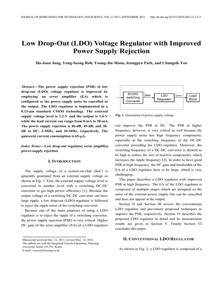
shown in Fig. 1. First, the external supply voltage level is
converted to another level with a switching DC-DC
converter to get high power efficiency [1]. Because the
output voltage of a switching DC-DC converter can have
large ripple, a low drop-out (LDO) regulator is followed
to reject the ripple noise of the switching converter.
Because one of the main purposes of using a LDO
regulator is to reject the ripple of a switching converter,
the power supply rejection (PSR) is very critical. Higher
DC gain of the error amplifier (EA) of a LDO regulator
Manuscript received Dec. 12, 2011; revised May. 14, 2012.
The authors are with the Integrated Circuits Laboratory, Hanyang
University, Seoul 133-791, Korea.
E-mail : csyoo@hanyang.ac.kr
Fig. 1. Generation of power supply voltage.
can improve the PSR at DC. The PSR at higher
frequency, however, is very critical as well because the
power supply noise has high frequency components,
especially at the switching frequency of the DC-DC
converter preceding the LDO regulator. Moreover, the
switching frequency of a DC-DC converter is desired to
be high to reduce the size of reactive components, which
increases the ripple frequency [2]. In order to have good
PSR at high frequency, the DC gain and bandwidth of the
EA of a LDO regulator have to be large, which is very
challenging.
This paper describes a LDO regulator with improved
PSR at high frequency. The EA of the LDO regulator is
composed of multiple stages which are designed so the
noise of the external power supply line can be cancelled
and does not appear at the output.
Section II and Section III review the conventional
LDO regulator and previously proposed techniques to
improve the PSR, respectively. Section IV describes the
proposed LDO regulator in detail and its measurement
results are given in Section V. Finally Section VI
concludes this paper.
II. CONVENTIONAL LDO REGULATOR
As shown in Fig. 2, a LDO regulator is composed of a
314
HO-JOON JANG et al : LOW DROP-OUT (LDO) VOLTAGE REGULATOR WITH IMPROVED POWER SUPPLY REJECTION
affecting the output. Because the gate capacitance of the
power transistor is generally very large, its gate node
voltage is free of ripple at high frequency and therefore
the supply noise coupling through the path 2 becomes
less problematic at high frequencies.
The gain of the path 3 is given as;
Vout
VDD
=
path 3
g mp Z out AEA
V
1 V
⋅ BGR ≈ ⋅ BGR .
1 + g mp Z out βAEA VDD
β VDD
(3)
From the above Eq. (3), it is clear the power supply noise
coupling through the path 3 is dominated by the PSR of
the bandgap reference circuit itself.
Fig. 2. Coupling paths of power supply noise to the output of
LDO regulator.
power transistor MP and EA which compares the
feedback voltage with the reference voltage VBGR. The
noise on the external power supply VDD can be coupled to
the output of the LDO regulator through the power
transistor (path 1), EA (path 2), and the reference voltage
(path 3) as shown in the figure.
The small-signal gain of the path 1 can be represented
as [3];
Vout
VDD
=
path1
g mp Z out
1 + g mp Z out βAEA
≈
1
.
βAEA
(1)
where gmp, Zout, β, and AEA are the transconductance of
the power transistor MP, load impedance at the output
node, feedback factor RFB2/(RFB1+ RFB2), and the gain of
the EA, respectively. From this equation, it can be seen
the power supply noise coupling through the path 1 is
determined by the feedback factor and the gain of the EA.
The PSR may be deteriorated at high frequency due to
the limited bandwidth of the EA.
The gain of the path 2 can be found in the same
manner as that of the path 1 and the result is;
Vout
VDD
=
path 2
g mp Z out AEA_VDD
1 + g mp Z out βAEA
≈
AEA_VDD
βAEA
.
(2)
where AEA_VDD is the gain from the power supply of the
EA to its output which is the gate of the power transistor.
The ripple of the power supply through the path 2 is first
coupled to the gate of the power transistor MP before
III. PREVIOUS TECHNIQUES FOR IMPROVED
POWER SUPPLY REJECTION
As described in the previous section, the power supply
noise can be coupled to the output of a LDO regulator
through multiple paths and therefore it is generally very
complicated to get a good PSR.
The simplest way of improving the PSR is to place a
low-pass RC filter on the external power supply line as
shown in Fig. 3(a) [4]. The RC filter reduces the ripple
noise of the external power supply before being delivered
to the input of the LDO regulator. The resistor of the RC
filter, however, causes the voltage drop on the power
supply line, which can make the design of LDO very
challenging. A common-gate nMOS transistor may be
inserted between the external power supply input and the
pMOS power transistor as shown in Fig. 3(b) [5]. The
nMOS transistor consumes voltage headroom and may
require large silicon area if the voltage headroom is to be
minimized.
In [6], the ripple on the external supply line is coupled
to the gate of the power transistor using a feed-forward
amplifier which equalizes the phase delay of the
compensating signal path with that of the main path of
the power supply noise coupling. However, the feedforward amplifier cannot perfectly equalize the phase
delay at all frequencies and operation conditions, which
limits the improvement of PSR.
In [7], the diode connected gain stage is inserted
between the power transistor and the error amplifier,
which injects the supply noise to gate of the power
transistor. The supply noise is not transferred to the
JOURNAL OF SEMICONDUCTOR TECHNOLOGY AND SCIENCE, VOL.12, NO.3, SEPTEMBER, 2012
(a)
315
output due to the unaffected gate-source voltage of the
power transistor. Because the diode connected gain stage
reduces the loop gain, the additional gain stage is
required, which requires a complex frequency compensation technique.
IV. POWER SUPPLY REJECTION (PSR)
IMPROVED LDO REGULATOR
(b)
(c)
(d)
Fig. 3. Power supply rejection improvement techniques with
(a) RC-filter on external supply line, (b) cascode transistor, (c)
feedforward ripple cancellation, (d) diode connected gain
stage.
The noise of the external power supply line can be
rejected if the exactly the same amount of noise can be
coupled to the gate of power transistor. This is the basic
background knowledge of the proposed LDO regulator
shown in Fig. 4. To perform the function, the diode
connected gain stage consisting of M7, and M8 uses a
power transistor driver, which reduces the loop gain and
regulation characteristics. The additional gain stage and
the bleeding current sources Ibleed1 and Ibleed2 are added to
increase voltage gain [8]. The EA of the LDO regulator
consisting of three stages is designed so the noise of the
external power supply line is cancelled.
The noise of the external supply is coupled to the
output of the first stage which drives the gate of the
pMOS transistor M5 [9]. Through this path, the supply
noise is delivered without much attenuation over a wide
frequency range because the parasitic capacitor of the
first stage output is not large. The output of the second
stage is free of the supply noise because the noises on the
gate and source nodes of the transistor M5 cancel each
other. Therefore, the output of the third stage is coupled
to the external power supply noise only by the transistor
M8. Because the transistor M8 is configured as a diode,
the output impedance of the third stage is very small and
the external power supply noise appears at the output of
the third stage without much attenuation over a wide
frequency range as well. The gate-source voltage of the
power transistor is free of the external power supply
noise and the PSR of the LDO regulator is improved.
The PSR of the proposed LDO regulator is derived as
in the Eq. (4) shown at the bottom of this page.
1 - 1 {1 + s ( CP 3 g m 8 )} + A2 ( s ) A3 ( s ) s ( ro 2 / /ro 4 ) CP1 {s ( ro 2 / /ro 4 ) CP1 + 1}
vOUT
( s ) = g mp ZTOT ( s ) ×
.
vDD
1 + g mp ZTOT ( s ) A1 ( s ) A2 ( s ) A3 ( s ) β ( s )
where A1 ( s ) =
g m1 (ro 2 //ro 4 )
gm5
gm7
RFB2
1
//RL , and β ( s ) =
, A2 ( s ) =
, A3 ( s ) =
, ZTOT ( s ) = β ( s ) //
.
1
g m 6 + sC P 2
g m8 + sC P 3
sCL
1 + s (ro 2 //ro 4 )CP1
RFB1 //
+ RFB 2
sCZ
(4)
316
HO-JOON JANG et al : LOW DROP-OUT (LDO) VOLTAGE REGULATOR WITH IMPROVED POWER SUPPLY REJECTION
Fig. 4. Proposed LDO regulator.
Fig. 5. Small-signal equivalent circuit of the proposed LDO
regulator for stability analysis.
(a)
Because the LDO regulator has four stages including
the power transistor, its stability has to be carefully
analyzed. The loop gain of the LDO regulator can be
derived with the small signal equivalent circuit shown in
Fig. 5 and the result is;
L (s ) =
g m1 (ro 2 //ro 4 )(g m 5 g m 6 )(g m 7 g m 8 )g mp R L β (s )
(1 + s (r
o2
sC P 2
//ro 4 )C p1 1 +
g m6
)
sC P 3
1 +
g m8
(1 + sR L C L )
.
(5)
The loop gain has four poles and one zero due to β(s)
in the loop gain as shown in the above Eq. (5). The
equivalent series resistor (ESR) RESR of the capacitor CL
is neglected because a ceramic capacitor is used which is
known to have small ESR. The pole at the LDO output P4
is the dominant pole of the loop. The poles at the outputs
P2 and P3 of the second and third stages can be neglected
because they are at high frequency. The zero generated
by the capacitor CZ compensates for the phase shift due
to the pole at the output of the first stage. The loop gain
(b)
Fig. 6. Simulated loop gain of the LDO regulator (a)
magnitude, (b) phase shift versus the frequency.
can be reduced to two poles and one zero system.
Therefore the proposed scheme does not require a large
compensation capacitor. The loop gain of the LDO
regulator is simulated for various values of load current
and the result is shown in Fig. 6.
JOURNAL OF SEMICONDUCTOR TECHNOLOGY AND SCIENCE, VOL.12, NO.3, SEPTEMBER, 2012
317
Bandgap Reference
Pass
Transistor
Error amp +
Small-gain stages
Fig. 9. Measured PSR for different load conditions.
Fig. 7. Microphotograph of the LDO regulator.
Fig. 10. Measured load transient response.
(a)
(b)
Fig. 8. Measured AC power under the condition of VDD=1.2 V
coupled with 1MHz and IL=30 mA at (a) input supply voltage,,
(b) output voltage.
V. MEASUREMENT RESULTS
The proposed LDO regulator has been implemented in
a 0.13-µm standard CMOS technology and the chip
microphotograph is shown in Fig. 7. The total area of the
LDO is 0.4-mm2. The output voltage is 1.0-V with the
nominal external supply voltage level 1.2-V and the load
current is from 0-mA to 50-mA. An off-chip ceramic
output capacitor 4.7-µF is used. The LDO regulator
including a bandgap reference circuit consumes only 65µA quiescent current.
To measure the PSR of proposed LDO, an AC coupled
supply voltage is fed into the LDO through Bias-T. The
PSR is calculated by subtraction of input and output AC
power as in [6]. Fig. 8 shows the measurement of the
input and output power at 1.2 V supply coupled with
1 MHz sine wave and load current of 30 mA. The
measured PSR for various load current conditions is
shown in Fig. 9. The minimum PSR is 46-dB at DC, 49dB at 2-MHz, and 38-dB at 10-MHz. The PSR at low
frequency is degraded for larger load current because the
loop gain is decreased. The load current is changed from
0-mA to 50-mA and vice-versa to see the ripple of the
output voltage due to the load transient. As shown in Fig.
10, the output voltage level changes by 15-mV and 18-
318
HO-JOON JANG et al : LOW DROP-OUT (LDO) VOLTAGE REGULATOR WITH IMPROVED POWER SUPPLY REJECTION
Table 1. Performance summary of the LDO regulator
[6]
[7]
This work
Technology [µm]
0.13
0.35
0.13
VDD [V]
1.15
3.1
1.2
VOUT [V]
1
2.8
1.0
Max. load current [mA]
25
100
50
Quiescent current [µA]
50
N.A.
65
Line regulation [mV/V]
N.A.
N.A.
4.25
Load regulation [mV/mA]
PSR [dB]
0.048
0.05
0.13
DC
60
70
46
2-MHz
80
N.A.
49
10-MHz
55
N.A.
38
mV for the change of load current from 0-mA to 50-mA
and from 50-mA to 0-mA, respectively. The performance
of the LDO regulator is summarized and compared with
other works in Table 1.
[3]
[4]
[5]
[6]
VI. CONCLUSIONS
The power supply rejection of a linear LDO regulator
is improved by configuring the error amplifier so the
power supply noise can be cancelled at the output. The
LDO regulator implemented in a 0.13-µm CMOS process
achieves 46-dB, 49-dB, and 38-dB power supply
rejection at DC, 2-MHz, and 10-MHz, respectively.
ACKNOWLEDGMENTS
This work was supported by the Seoul R&BD
Program (SS100022) and Basic Science Research
Program through the National Research Foundation of
Korea (NRF) funded by the Ministry of Education,
Science, and Technology (2010-0012551). The chip
fabrication is supported by the IC Design Education
Center (IDEC).
[7]
[8]
[9]
[10]
3131–3145, Nov. 2009.
P. K. T. Mok, “Embedded Power Management
Circuits,” in IEEE Int. Solid-State Circuits Conf.
(ISSCC) Tutorials T1, Feb. 2007.
“Application Note 883: Improved Power Supply
Rejection for IC Linear Regulators,” Maxim
Integrated Products, Inc., Sunnyvale, CA, Oct.
2002 [Online]. Available: http://www.maximic.
com/ appnotes.cfm/ appnote_number/883, accessed
on Dec. 4, 2008.
J. M. Ingino and V. R. von Kaenel, “A 4-GHz
clock system for a high-performance system-on-achip design,” IEEE J. Solid-State Circuits, pp.
1693-1698, Nov. 2001.
M. El-Nozahi, A. Amer, J. Torres, K. Entesari and
E. Sanchez-Sinencio, “High PSR Low Drop-Out
Regulator with Feed-Forward Ripple Cancellation
Technique,” IEEE J. Solid-State Circuits, vol. 45,
pp. 565-577, Mar. 2010.
S. K. Hoon, S. Chen, F. Maloberti, J. Chen, B. Aravind,
“A Low Noise, High Power Supply Rejection Low
Dropout Regulator for Wireless System-on-Chip
Applications,” IEEE Custom Integrated Circuits
Conference, pp. 759-762, Sep. 2005.
B. Razavi, Design of Analog CMOS Integrated
Circuits, McGraw-Hill, New York, International
Edition 2001.
V. Gupta, G. A. Rincon-Mora and P. Raha,
“Analysis and Design of Monolithic, High PSR,
Linear Regulator for SoC Applications,” IEEE Intl.
SoC Conf., pp. 311-315, Sep. 2004.
V. Gupta and G. A. Rincon-Mora, “A 5mA 0.6um
CMOS Miller-Compensated LDO regulator with27dB worst-case power-supply rejection using
60pF of on-chip capacitance,” in IEEE Int. SolidState Circuits Conf. (ISSCC) Dig. Tech. Papers, pp.
520-521, Feb. 2007.
REFERENCES
[1]
[2]
A. J. Stratakos, S. R. Sanders, and R. W. Broderson,
“A low-voltage CMOS dc-dc converter for a portable
battery-operated system,” in Proc. Power Electronics
Specialists Conf., vol. 1, pp. 619-626, Jun. 1994.
P. Li, P. Hazucha, T. Karnik, and R. Bashirullah,
“A delay locked loop synchronization scheme for
high frequency multiphase hysteretic DC-DC
converter,” IEEE J. Solid-State Circuits, vol. 11, pp.
Ho-Joon Jang received the B.S.
degree in electrical and computer
engineering in 2010 and the M.S.
degree in information display engineering in 2012, both from Hanyang
University, Seoul, Korea. He joined
Samsung Electro-Mechanics, Suwon,
Korea, in 2012. His research interests include power
management integrated circuit design.
JOURNAL OF SEMICONDUCTOR TECHNOLOGY AND SCIENCE, VOL.12, NO.3, SEPTEMBER, 2012
Yong-Seong Roh received the B.S.
(with the highest honor) degree from
Hanyang University, Seoul, Korea, in
2007, and is currently working
toward the Ph.D. degree at Hanyang
University. His research interests
include power management integrated circuit design.
Young-Jin Moon received the B.S.
degree in electrical and computer
engineering from Hanyang University,
Seoul, Korea, in 2008, and is
currently working toward the Ph.D.
degree at Hanyang University. His
research interests include power
management integrated circuit design.
Jeongpyo Park received the B.S.
degree in electronics and computer
engineering from Hanyang University,
Seoul, Korea, in 2011, and is
currently working toward the Ph.D.
degree at Hanyang University. His
research interests include power
management integrated circuit design.
319
Changsik Yoo received the B.S.
(with the highest honor), M.S., and
Ph.D. degrees from Seoul National
University, Seoul, Korea, in 1992,
1994, and 1998, respectively, all in
electronics engineering. From 1998
to 1999, he was with Integrated
Systems Laboratory (IIS), Swiss Federal Institute of
Technology (ETH), Zurich, Switzerland, as a Member of
Research Staff working on CMOS RF circuits. From 1999
to 2002, he was with Samsung Electronics, Hwasung,
Korea. Since 2002, he has been a Professor of Hanyang
University, Seoul, Korea. From 2008 to 2009, he was with
Silicon Image Inc. Sunnyvale, California as a Senior
Engineer to develop a HDMI receiver IC during the
sabbatical leave. His main research interests include
mixed-mode CMOS circuit, high-speed interface circuit,
and power management integrated circuit. Dr. Yoo is the
winner or co-winner of several technical awards including
Samsung Best Paper Bronze Award in 2006 International
SoC Design Conference, Silver Award in 2006 IDEC Chip
Design Contest, Best Paper Award in 2006 Silicon RF IC
Workshop, and Golden Prize for research achievement in
the next-generation DRAM design from Samsung
Electronics in 2002. He served as a member of technical
committee of IEEE Int. Solid-State Circuits Conference
(ISSCC) and is serving as a member of technical
committee of VLSI Circuits Symposium (SOVC) and
European Solid-State Circuits Conference (ESSCIRC).


