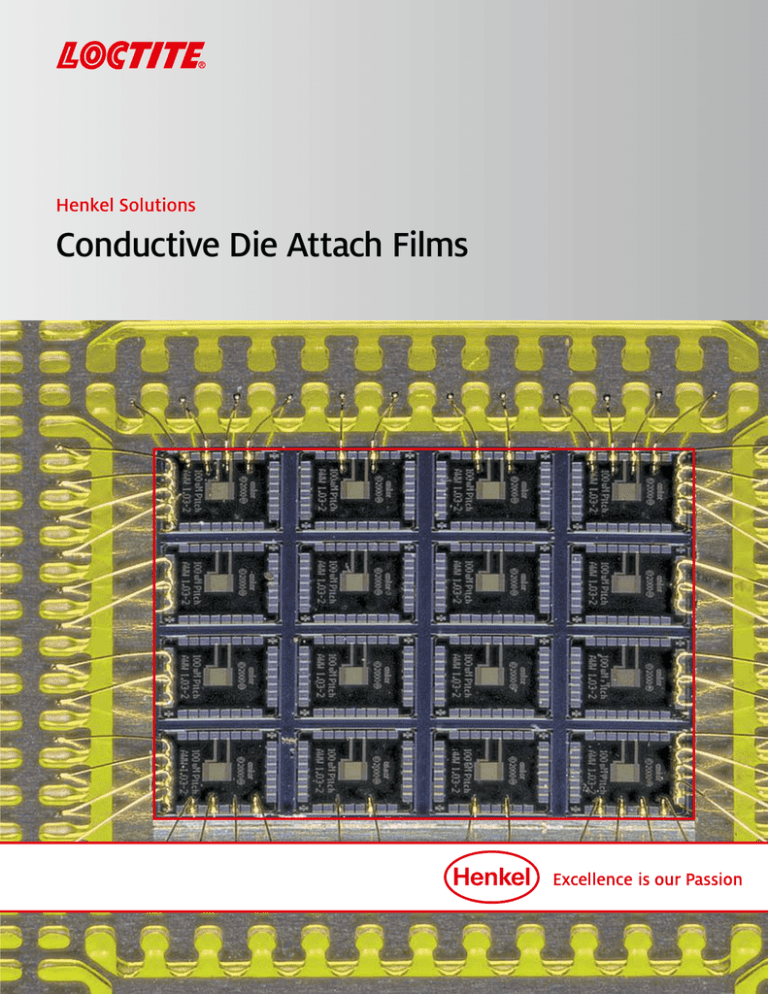
Henkel Solutions
Conductive Die Attach Films
Conductive Die Attach Film
Henkel was the first to develop and introduce conductive die attach film (CDAF) to the
semiconductor market. A groundbreaking market development, this innovation was
viewed by the semiconductor industry as a significant breakthrough that would enable
more capable and cost-effective lead frame package designs. Indeed, this has been the
result, as numerous semiconductor packaging specialists have leveraged Henkel’s CDAF
advantages for new and better package designs.
LOCTITE® ABLESTIK C100 was the premier material in Henkel’s CDAF line, and, since
then, the company has expanded the suite of conductive films to address various lead
frame and laminate package requirements. Each material offers different properties
and characteristics – from dicing die attach capability to varying thermal and electrical
performance to cost competitiveness – but all of them deliver the undeniable
advantages of film-based materials over that of conventional die attach paste.
Some of the most notable comparable benefits of film vs. paste are:
• Design flexibility and ability to integrate more die per package due to tight clearance
between the die and die pad
• Allows for thinner packages with higher densities
• Facilitates thin-wafer handling
• Provides for a clean process with no bleed, uniform bondlines and no kerf creep
Consumers continue to demand ever smaller and more capable devices, and Henkel’s
CDAF materials are making this ongoing product dynamic possible.
Paste with Fillet
Film with Controlled Fillet
Conductive film technology enables
tighter die-to-pad ratio
Package Trends – Wire Bonded
Higher functionality and efficiency
Miniaturized Packages (QFN, DFN, SOs)
Higher Density Packages
•Increased die-to-pad ratio
• Multi-die packages
•In some cases, D/P ratio close to 1.0
• SiP – LGA/PBGA
Thinner Packages (QFN, SO, QFP)
•Packages < 0.3mm
•Thinner die < 75µm
•Thinner DA bondline thickness < 20µm
Current Material Challenges on Lead Frames
Conducting die attach paste
•Dispensing: Optimize dispense patterns for various die sizes – 0.2mm x 0.2mm to > 10mm x 10mm
•Fillet & Bleed: Forces engineers to have a minimum keep out zone around die
•Bondline Control: Especially for smaller die, BLT control is challenging and leads to die tilt
•Kerf Creep: For thinner wafers, uneven fillet height can lead to kerf creep
Control Flow Solutions
Enables miniaturization
Reduces Footprint
• Shorter interconnection
• Faster signal speed
•Less Au wire, lead frame and EMC used
• Lower TCoO
Henkel’s Solution to Control Flow
Product space
Higher electrical (RDSon) and
thermal (Rth) performance
A4: Low warpage, ultra-high thermal, MSL1, < 15µm thick
CDF 800P
MSL2 on all LF finish
CDF 200P
CDF 500P
CDF 500P
MSL1 on all LF finish
MSL2 on Laminates
L: QFN
2mm x 2mm
CDF 600P
4mm x 4mm
6mm x 6mm
Die Size
8mm x 8mm
Thermal and Electrical for CDAF
Stable in-package performance
•Thermal Conductivity (W/mK) is an intrinsic material property
•Thermal Resistance, Rth (K/W), is a geometry-dependent value that allows us to better compare materials in a
functional package
•70% - 90% of the Rth is due to the interfaces and is not captured in thermal conductivity values
Thermal Resistance (Rth)
Comparison of paste and film materials
3.0
2.5
2.5 x 2.5 x 0.36mm2 Si-back die
QFN 7 x 7mm, PPF (pad 5.8 x 5.8mm)
30 min ramp to 200˚C + 1 hr cure
Rth(K/W)
2.0
1.5
1.0
CDF 500P
11
3.5
6.5
1-27.8 1
2100A
QMI529HT
CDF 600P
CDF 800P
1.6
FS 849-TI
8008HT
2.5
8290
84-1LMISR4
3.8
QMI519
2
0
CDF 200P
.5
1
Thermal Conductivity (W/mK)
Electrical Resistance RDSon
In-package performance
0.08
2.0 x 2.9 x 0.18mm; TiNiAg-back die
TO-220, Cu pad
0.07
RDSon (ohm)
0.06
0.05
0.04
0.03
0.02
CDF
QMI519
84-1LMISR4
8008HT
CDF
QMI529HT
200P 800P
CDF
FS 500P849-TI
Portfolio of CDAF Products
Film and paste performance comparison
UNIT
CDF
200P
QMI519
84-1LMISR4
8290
8008HT
CDF
800P
QMI529HT
CDF
500P
FS
849-TI
CDF
600P
2100A
ohm-cm
0.0014
0.0001
0.0002
0.008
0.00006
0.0003
0.00004
0.0002
0.00002
0.0008
0.05
Thermal Conductivity
W/mK
2
3.8
2.5
1.6
11
3.5
6.5
1-2
7.8
1
1.35
CTE Alpha1
ppm/C
48
40
40
81
37
40
53
60
44
75
65
CTE Alpha2
ppm/C
120
140
150
181
62
118
156
245
155
320
200
Glass Transition
Temperature
˚C
15
75
120
38
264
11
3
10
211
-5
60
Modulus @ 25˚C
MPa
5,400
5,300
3,930
3,034
6,659
7,100
3,300
6,300
7,800
3,000
3,200
Modulus @ 250˚C
MPa
1,000
284
303
117
2,450
900
-
130
1,070
40
230
HDSS (260˚C) on Ag
kg/mm2
1.3
0.8
0.2
0.6
0.7
1.0
0.5
0.7
0.5
0.7
0.4
Room Temp DSS on PPF
kg/mm2
2.14
4.9
3.0
5.0
-
> 2.0
-
-
-
-
-
Room Temp DSS on Ag
kg/mm2
3.02
4.8
2.3
5.1
1.5
> 2.0
2.2
-
-
-
-
Room Temp DSS on Cu
kg/mm2
3.17
1.8
1.2
2.5
1.5
> 2.0
-
-
-
-
-
Cohesive
Cohesive
-
Cohesive
Cohesive
Cohesive
-
Cohesive
Cohesive
MATERIAL PROPERTY
Volume Resistivity
PERFORMANCE
Failure Mode
Thermal Resistance, Rth
Cohesive Cohesive
K/W
1.5
1.3
0.83
1.8
1.5
0.81
0.77
1.5
0.72
2.1
2.3
ohm-cm
0.075
0.044
0.033
n/a
0.067
0.032
0.042
0.055
0.038
n/a
n/a
RDSon Shift (500 TC)
%
2.2
n/a
10.0
n/a
n/a
5.7
42.0
n/a
28.0
n/a
n/a
RDSon Shift (1,000 TC)
%
6.6
n/a
15.6
n/a
n/a
6.4
42.0
n/a
28.8
n/a
n/a
3
MSL1
capable
for
small
die
3
1
MSL1
capable
for
small
die
1
MSL1
capable
for
small
die
2
(PBGA)
2
(PBGA)
-
-
-
2
-
1
3
2
(PBGA)
2
(PBGA)
30 min
ramp to
175˚C +
30 min
soak @
175˚C
30 min
ramp to
100˚C +
30 min
soak @
100˚C +
30 min
ramp to
200˚C +
60 min
soak @
200˚C
30 min
ramp to
175˚C +
15 min
soak @
175˚C
RDSon
JEDEC MSL 260˚C
(on 7 x 7mm PPF QFN with
2.5 x 2.5 x 0.33mm die)
MSL
level
1
MSL1
capable
for
small
die
JEDEC MSL 260˚C
(on 7 x 7mm PPF QFN
with 5 x 5 x 0.36mm die)
MSL
level
2
-
30 min
ramp to
200˚C
+ 60
min
soak @
200˚C
30 min
ramp +
hold 60
min @
100˚C +
15 min
ramp +
hold 60
min @
200˚C
PROCESSING
Cure
profile
30 min ramp
to 175˚C +
60 min soak
@ 175˚C
30 min
ramp to
175˚C +
15 min
soak @
175˚C
20 sec @
280˚C
30 min
ramp to
200˚C
+
60 min
soak @
200˚C
30 min ramp
to 185˚C +
30 min soak
@ 185˚C
30 min
ramp to
200˚C
+
60 min
soak @
200˚C
AMERICAS
ASIA-PACIFIC
HEADQUARTERS:
CHINA
No. 332 Meigui South Road
WaiGaoQiao Free Trade Zone
Shanghai 200131, P.R. China
Tel: +86.21.3898.4800
Fax: +86.21.5048.4169
UNITED STATES
Henkel Electronic Materials LLC
14000 Jamboree Road
Irvine, CA 92606
USA
Tel: +1.714.368.8000
Tel: +1.800.562.8483
Customer Support: +1.888.943.6535
Fax: +1.714.368.2265
Henkel Electronic Materials LLC
20021 Susana Road
Rancho Dominguez, CA 90221
USA
Tel: +1.310.764.4600
Fax: +1.310.605.2274
BRAZIL
Henkel Brazil
Av. Prof. Vernon Krieble, 91
06690-250 Itapevi,
Sao Paulo, Brazil
Tel: +55.11.3205.7000
EUROPE
BELGIUM
Henkel Electronic Materials (Belgium)
Nijverheidsstraat 7
B-2260 Westerlo
Belgium
Tel: +32.1457.5611
Fax: +32.1458.5530
Henkel Huawei Electronics CO. LTD
Songtiao Industrial Park Lianyungang
Jiangsu Province 222006 China
Tel: +86.518.8515.5336
Fax: +86.518.8515.3801
JAPAN
Henkel Japan Ltd.
27-7, Shin Isogo-cho
Isogo-ku Yokohama, 235-0017
Japan
Tel: +81.45.758.1900
KOREA
Henkel Technologies (Korea) Ltd.
6th Floor
Dae Ryung Techno Town II
569-21 Gasan-dong,
Geumcheon-gu, Seoul 153-771
Korea
Tel: +82.2.6675.8000
MALAYSIA
Henkel (Malaysia) Sdn. Bhd
Lot 62049, Jalan Portland,
Tasek Industrial Estate,
31400 Ipoh, Perak, Malaysia
Tel : +605-5476811
Fax: +605-5471868
TAIWAN
Henkel Taiwan Ltd
Room A4, 19F-1, No.6, Sihwei 3rd Rd,
Lingya Dist., Kaohsiung, Taiwan
Tel: 886-7-335-7970
Fax: 886-7-335-1057
Across the Board,
Around the Globe.
www.henkel.com/electronics
All marks used above are trademarks and/or registered trademarks of Henkel and its affiliates in the U.S., Germany and elsewhere.
© 2014 Henkel Corporation. All rights reserved. 12016/LT-6901 (3/14)
