CMOS RF Modeling and Parameter Extraction Approaches Taking
advertisement

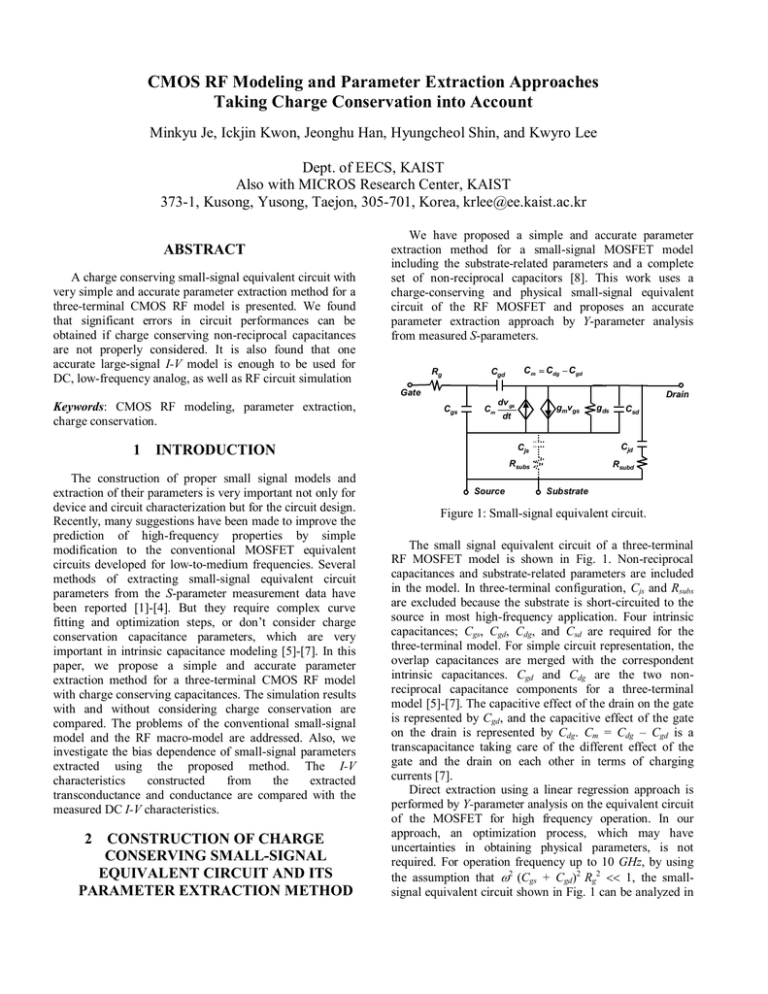
CMOS RF Modeling and Parameter Extraction Approaches Taking Charge Conservation into Account Minkyu Je, Ickjin Kwon, Jeonghu Han, Hyungcheol Shin, and Kwyro Lee Dept. of EECS, KAIST Also with MICROS Research Center, KAIST 373-1, Kusong, Yusong, Taejon, 305-701, Korea, krlee@ee.kaist.ac.kr ABSTRACT A charge conserving small-signal equivalent circuit with very simple and accurate parameter extraction method for a three-terminal CMOS RF model is presented. We found that significant errors in circuit performances can be obtained if charge conserving non-reciprocal capacitances are not properly considered. It is also found that one accurate large-signal I-V model is enough to be used for DC, low-frequency analog, as well as RF circuit simulation We have proposed a simple and accurate parameter extraction method for a small-signal MOSFET model including the substrate-related parameters and a complete set of non-reciprocal capacitors [8]. This work uses a charge-conserving and physical small-signal equivalent circuit of the RF MOSFET and proposes an accurate parameter extraction approach by Y-parameter analysis from measured S-parameters. Cm = Cdg − Cgd Cgd Rg Gate Keywords: CMOS RF modeling, parameter extraction, charge conservation. Cgs Cm 2 CONSTRUCTION OF CHARGE CONSERVING SMALL-SIGNAL EQUIVALENT CIRCUIT AND ITS PARAMETER EXTRACTION METHOD gmvgs dt 1 INTRODUCTION The construction of proper small signal models and extraction of their parameters is very important not only for device and circuit characterization but for the circuit design. Recently, many suggestions have been made to improve the prediction of high-frequency properties by simple modification to the conventional MOSFET equivalent circuits developed for low-to-medium frequencies. Several methods of extracting small-signal equivalent circuit parameters from the S-parameter measurement data have been reported [1]-[4]. But they require complex curve fitting and optimization steps, or don’t consider charge conservation capacitance parameters, which are very important in intrinsic capacitance modeling [5]-[7]. In this paper, we propose a simple and accurate parameter extraction method for a three-terminal CMOS RF model with charge conserving capacitances. The simulation results with and without considering charge conservation are compared. The problems of the conventional small-signal model and the RF macro-model are addressed. Also, we investigate the bias dependence of small-signal parameters extracted using the proposed method. The I-V characteristics constructed from the extracted transconductance and conductance are compared with the measured DC I-V characteristics. Drain dv gs Source gds Csd Cjs Cjd Rsubs Rsubd Substrate Figure 1: Small-signal equivalent circuit. The small signal equivalent circuit of a three-terminal RF MOSFET model is shown in Fig. 1. Non-reciprocal capacitances and substrate-related parameters are included in the model. In three-terminal configuration, Cjs and Rsubs are excluded because the substrate is short-circuited to the source in most high-frequency application. Four intrinsic capacitances; Cgs, Cgd, Cdg, and Csd are required for the three-terminal model. For simple circuit representation, the overlap capacitances are merged with the correspondent intrinsic capacitances. Cgd and Cdg are the two nonreciprocal capacitance components for a three-terminal model [5]-[7]. The capacitive effect of the drain on the gate is represented by Cgd, and the capacitive effect of the gate on the drain is represented by Cdg. Cm = Cdg – Cgd is a transcapacitance taking care of the different effect of the gate and the drain on each other in terms of charging currents [7]. Direct extraction using a linear regression approach is performed by Y-parameter analysis on the equivalent circuit of the MOSFET for high frequency operation. In our approach, an optimization process, which may have uncertainties in obtaining physical parameters, is not required. For operation frequency up to 10 GHz, by using the assumption that ω2 (Cgs + Cgd)2 Rg2 << 1, the smallsignal equivalent circuit shown in Fig. 1 can be analyzed in terms of Y-parameters [8]. The validity of the assumption will be checked after each parameter is extracted. All the components of the equivalent circuit are extracted by the Y-parameter analysis. gm is obtained from the y-intercept of Re(Y21) versus ω2 and gds is extracted from the y-intercept of Re(Y22) versus ω2, at the low frequency range. Rg, Cgd, Cgs and Cdg can be obtained by (1)–(4). R g = Re(Y11 ) /(Im(Y11 )) 2 (1) C gd = − Im(Y12 ) / ω (2) C gs = (Im(Y11 ) + Im(Y12 )) / ω (3) C dg = − Im(Y21 ) / ω − g m R g (C gs + C gd ) (4) vector network analyzer. To remove on-wafer pad parasitics, a two-step deembedding was carried out by using the open and short deembedding structures. The parameters were extracted for an n-MOSFET with 100-µm width having forty gate fingers. 48.5 mS 3.2 mS 8.4 Ω 43.3 fF 109.6 fF 71.5 fF 69.4 Ω 82.7 fF -16.8 fF gm gds Rg Cgd Cgs Cdg Rsubd Cjd Csd Table 1: Summary of extraction results. For the extraction of substrate components Rsubd and Cjd, Ysub is first defined as follows: Ysub = Y22 − g ds − ω 2 C gd C dg R g − ω 2 g m R g2 C gd (C gs + C gd ) − jωC sd − jωC gd − jωg m R g C gd = ω 2 C jd 2 Rsubd 1 + ω C jd Rsubd 2 2 2 + jωC jd 1 + ω C jd Rsubd 2 2 (5) 2 All the small signal parameters were extracted at Vgs = 1 V and Vds = 1 V. The extracted values of all parameters were summarized in Table 1. Due to the non-reciprocity, Cdg is larger than Cgd as it should be. For the extracted parameter values, ω2 (Cgs + Cgd)2 Rg2 is calculated to be 0.065 even at 10 GHz, which is much smaller than one. This confirms the validity of the assumption used for deriving (1)–(8). Rsubd is obtained from the slope of the relationship for ω2/Re(Ysub) vs. ω2 by (6). 12 Measured Proposed model ω2 = ω R subd + 1 2 Re(Ysub ) (6) 2 C jd R subd Y11 [mA/V] 10 Cjd is obtained from the following. 8 Im[Y11] W/L= 40x2.5 / 0.18 Vgs=1V, Vds=1V 6 (a) 4 2 ω C jd = 2 R subd Re(Y ) sub Re[Y11] −1 / 2 − ω 2 R subd 2 0 (7) 0 2 4 6 8 10 Frequency [GHz] 0.5 Finally, Csd is obtained from (8) as Im(Y22 ) ω − C gd − C jd 1 + ω 2 C jd 2 R subd 2 + ω 2 C gd C dg (C gd + C gs ) R g − g m R g C gd 2 (8) Y12 [mA/V] C sd = 0.0 Re[Y12] -0.5 -1.0 -1.5 -2.0 3 MODEL VERIFICATION The proposed direct extraction method was applied to determine parameters of the test device, which is a multifingered n-MOSFET fabricated by 0.18 µm technology. Sparameters were measured in the common source-substrate configuration using on-wafer RF probes and a HP 8510C Measured Proposed model -2.5 -3.0 (b) W/L= 40x2.5 / 0.18 Vgs=1V, Vds=1V 0 2 4 Im[Y12] 6 Frequency [GHz] 8 10 50 Re[Y21] Y21 [mA/V] 40 Measured Proposed model 30 20 (c) W/L= 40x2.5 / 0.18 Vgs=1V, Vds=1V 10 Im[Y21] 0 -10 0 2 4 6 8 10 Frequency [GHz] 8 Y22 [mA/V] Im[Y22] Measured Proposed model 7 6 W/L= 40x2.5 / 0.18 Vgs=1V, Vds=1V 5 Im(Y21) & Im(Y12) [mA/V] feedback drain-to-gate capacitances, which are very important for RF circuit design. Inaccuracy in capacitance can significantly affect the matching condition, gain, stability, noise figure, oscillation frequency, and so on. Fig. 2 demonstrates that the model with charge conserving capacitances can accurately fit both Im(Y12) and Im(Y21). 60 -2 -6 2 0 2 4 6 8 measurement [1] macro-model -10 0 2 Im(Y21) 4 6 8 10 Frequency [GHz] Figure 3: Im(Y12) and Im(Y21) from the models (a model of [1] and a macro-model) and the measurement. (d) 1 W/L= 40x2.5 / 0.18 Vgs=1V, Vds=1V -8 Re[Y22] 3 Im(Y12) -4 -12 4 0 0 10 D Frequency [GHz] Cgdx Figure 2: Modeled Y-parameters vs. measured Yparameters: (a) Y11, (b) Y12, (c) Y21, (d) Y22. Rg Gext G B Cgsx Rsub Bext Cjs S Figure 4: RF macro-model. 4 BIAS DEPENDENCE OF THE EXTRACTED PARAMETERS 140 120 Capacitance [fF] In Fig. 2, the Y-parameters calculated with extracted parameters are compared with the measured data for Vgs = 1 V and Vds = 1 V. It shows that the simulation result well matches the measurement without any optimization after direct extraction. The non-reciprocal capacitances Cgd and Cdg contribute to the imaginary parts of Y12 and Y21. Excluding transcapacitance could result in a significant error on the imaginary part of Y21 at high frequencies. The substrate coupling significantly contributes to the output admittance Y22 at high frequencies. The total root-meansquare error between measured and modeled Y-parameters is only 1.8 %. In Fig. 3, we compared the Im(Y12) and Im(Y21) from the conventional small-signal model [1] and the macro-model (Fig. 4) with the measured ones. The model parameters for these models were carefully extracted to best fit the measurement data. The small-signal model in [1] is very simple and doesn’t have a complete set of charge conserving capacitances, which results in large discrepancy in Im(Y21). We used the RF macro-model in Fig. 4. External Cgsx and Cgdx are added to describe the bias dependence of the overlap capacitance. These external capacitances also allow one to correct the inaccuracies of the intrinsic capacitances appearing for short-channel devices. However, with the reciprocal capacitance Cgd, we cannot simultaneously correct Cgd and Cdg (and thus, Im(Y12) and Im(Y21)) as shown in Fig. 3. It also means that we cannot simultaneously fit both the feedforward gate-to-drain and Cjd 100 W/L= 40x2.5 / 0.18 Vds=1V Cgs Cdg 80 60 Cgd 40 Cm 20 0 (a) -20 0.0 0.2 0.4 0.6 0.8 1.0 1.2 1.4 1.6 1.8 2.0 Vgs [V] 120 Cgs Capacitance [fF] 100 80 Cdg 60 40 Cgd 20 Cm W/L= 40x2.5 / 0.18 Vgs=1V 0 (b) -20 0.0 0.2 0.4 0.6 0.8 1.0 1.2 1.4 1.6 1.8 2.0 Vds [V] The extracted gds values at Vgs =1 V and 1.5 V were plotted as a function of Vds in Fig. 6(a) with the result from DC measurement while Fig. 6(b) shows Id-Vds curves generated by integrating the extracted gds and the curves from DC measurement. Similar results were obtained for gm vs. Vgs and Id vs Vgs. The results from S-parameter measurement at high-frequencies agree well with those from DC measurement. Therefore, one large-signal I-V model is enough to be used for DC, low-frequency analog, as well as RF circuit simulation. Thus one should not worry about path independence in constructing large signal based on integration of measured small signal conductance data [7]. 5 CONCLUSIONS Figure 5: Bias dependence of capacitances: (a) gate bias dependence, (b) drain bias dependence. Fig. 5 shows the bias dependence of the extracted capacitances; (a) for the gate bias dependence and (b) for the drain bias dependence. Note that the C-V behavior is what we expect from MOSFET device physics and specifically that Cdg is larger than Cgd , demonstrating the necessity of considering transcapacitance of Cm. This consideration of charge conservation is important not only for the accuracy in circuit simulation but also for the compatibility with large signal Q-V models [5]-[7]. A charge conserving small signal equivalent circuit with very simple and accurate parameter extraction method for a three-terminal CMOS RF model was introduced. The parameters can be extracted directly from the real and imaginary parts of Y-parameters. Without any complex fitting or optimization step, the total root-mean-square error between the modeled and measured Y-parameters is only 1.8 %. The necessity of proper consideration for charge conservation is emphasized not only for accuracy in RF circuit simulation but also for compatibility with large signal Q-V models. Lastly it is found that one accurate large-signal I-V model is enough to be used for DC, lowfrequency analog, as well as RF circuit simulation. 0.12 ACKNOWLEDGEMENTS W/L= 40x2.5 / 0.18 gds [mA/V] 0.10 DC IV measurement from extracted gds 0.08 This work was supported by MICROS research center, Silvaco International, and the National Program for TeraLevel Nano-Devices through MOST. Vgs=1.5V 0.06 0.04 REFERENCES (a) 0.02 Vgs=1V 0.00 0.0 0.2 0.4 0.6 0.8 1.0 1.2 1.4 1.6 1.8 Vds [V] 50 W/L= 40x2.5 / 0.18 40 Id [mA] Vgs=1.5V 30 DC IV measurement from extracted gds 20 Vgs=1V 10 (b) 0 0.0 0.2 0.4 0.6 0.8 1.0 1.2 1.4 1.6 1.8 Vds [V] Figure 6: DC measurement vs. extracted results from Sparameters: (a) gds vs. Vds, (b) Id vs. Vds. [1] D. Lovelace, J. Costa, and N. Camilleri, IEEE MTTS, 865-868, 1994. [2] G. D. Dambrine, A. Cappy, F. Helidore, and E. Palyze, IEEE TMTT, 36, 173-176, 1998. [3] R. Sung, P. Bendix, and M. B. Das, IEEE TED, 45, 1769-1775, 1998. [4] S. Lee, H. K. Yu, C. S. Kim, J. G. Koo, and K. S. Nam, IEEE MGWL, 7, 75-77, 1997. [5] P. Yang, B. D. Epler, P. K. Chatterjee, IEEE JSSC, SC-18, 1983. [6] Y. Tsividis, “The Operation and Modeling of the MOS Transistor,” McGraw-Hill, 1987 [7] D. E. Root and S. Fan, IEEE MTT-S, 255--258, 1992. [8] I. Kwon, M. Je, K. Lee, and H. Shin, ESSCIRC, 296-299, 2000.


