news & views
devices. Furthermore, separation and
recombination of photoinduced electron–
hole pairs at a heterojunction interface
are primary mechanisms governing the
operation of solar cells, photodetectors
and light-emitting devices. Both Gong and
collaborators and Duan and colleagues
managed to electrically address the lateral
heterojunctions and perform transport
measurements to investigate their electrical
behaviour. Even though the contacted
structures are not predefined in shape
and thus are far from optimized devices,
rectifying behaviour across the junctions
was clearly observed, showing a concrete
proof of principle. Both groups also showed
clear evidence of the photoresponse of
the heterojunctions in their transport
measurements. Similarly, charge
recombination at the lateral heterojunctions
has been characterized in the three
studies by means of photoluminescence
imaging, which revealed an enhanced
emission response at the interline between
the materials in all cases. Mastering the
in-plane growth of different TMDs down
to the single-atom level could enable the
synthesis of laterally quantum-confined
systems, with promise of exciting physics.
Also, this could open up opportunities
for a wide range of devices, including
complementary logic circuits, highfrequency devices and photodetectors.
Whereas the lateral junctions show scope
for miniaturization, the development of
larger scale vertical heterojunctions will
prove crucial for commercial applications
in light emission and light harvesting.
Large-scale photodiodes using vapourphase-grown MoS2 transferred to silicon
wafers have been realized already 12. They
have shown impressive performance and
have also revealed that using vapour-phasegrown materials allows tuning of the optical
response of the device. However, the in situ
growth of a bilayer heterojunction could
largely improve on this, in particular by
engineering pristine interfaces that are not
achievable by transfer techniques. Further
optimization of the CVD process will lead
to better control over the grown structures
and over the interface quality. Future work
will extend these approaches towards other
material sets with arresting discoveries
yet to come.
❐
Georg S. Duesberg is at the Centre for Adaptive
Nanostructures and Nanodevices (CRANN) and
the Advanced Materials BioEngineering Research
Centre (AMBER), School of Chemistry, Trinity
College Dublin, Dublin 2, Ireland.
e-mail: duesberg@tcd.ie
References
1.
2.
3.
4.
Geim, A. K. Science 324, 1530–1534 (2009).
Novoselov, K. S. et al. Nature 438, 197–200 (2005).
Geim, A. K. & Grigorieva, I. V. Nature 499, 419–425 (2013).
Radisavljevic, B. & Kis, A. Nature Mater.
12, 815–820 (2013).
5. Fang, H. et al. Proc. Natl Acad. Sci. USA 111, 6198–6202 (2014).
6. Pospischil, A., Furchi, M. M. & Mueller, T. Nature Nanotech.
9, 257–261 (2014).
7. Roy, K. et al. Solid State Commun. 175–176, 35–42 (2013).
8. Gong, Y. et al. Nature Mater. 13, 1135–1142 (2014).
9. Huang, C. et al. Nature Mater. 13, 1096–1101 (2014).
10.Duan, X. et al. Nature Nanotech. http://dx.doi.org./10.1038/
nnano.2014.222 (2014).
11.Miyata, Y. et al. Appl. Phys. Express 5, 085102 (2012).
12.Yim, C. et al. Sci. Rep. 4, 5458–5462 (2014).
2D CRYSTAL SEMICONDUCTORS
Intimate contacts
High electrical contact resistance had stalled the promised performance of two-dimensional layered devices.
Low-resistance metal–semiconductor contacts are now obtained by interfacing semiconducting MoS2 layers with
the metallic phase of this material.
Debdeep Jena, Kaustav Banerjee and Grace Huili Xing
T
ransistors and lasers made of
semiconductor materials power the
information age by providing the
building blocks for electronic switching,
amplification and photonic communication.
The electronic and photonic properties
of the semiconductor play a primary role
in determining the performance of such
devices, yet comparable importance resides
in the way this material interfaces with the
external metallic circuits. A high electrical
resistance due to a high energy barrier —
the Schottky barrier — encountered by the
charge carriers moving through the metal–
semiconductor contacts saps the energy
efficiency, and significantly degrades the
performance of the device.
Semiconductor researchers are
excited about the potential of transition
metal dichalcogenide (TMD) layered
semiconductors. For device applications,
the excitement is fuelled by the dream
of improving device performance by
1076
using a semiconductor channel that is
potentially one monolayer thick1. The first
generation of field-effect transistors made
from MoS2 and related TMDs have shown
promise, but trail the silicon and III–V
semiconductor analogues significantly in
performance. A high contact resistance is
the root cause. Writing in Nature Materials,
Rajesh Kappera and colleagues now report
an unconventional method to address
this problem head-on2, based on the local
conversion of MoS2 semiconducting layers
into a metal that lowers the barrier to the
charges flowing in the external circuits.
The traditional method to lower the
contact resistance between a metal and a
semiconductor relies on an intermediate
layer, usually a heavily doped semiconductor
that helps charge carriers from the metal
to be injected in the conduction and
valence bands of the semiconductor. The
metal is chosen based on its workfunction,
so that it creates a low Schottky barrier
height with the semiconductor contact
region, whereas heavy doping reduces
the thickness of the barrier, enabling a
significant fraction of electrons to quantum
mechanically tunnel through it. However,
chemical doping has proven challenging
with TMD semiconductors. In their work,
Kappera et al. exploit the fact that MoS2
exists in two crystalline phases: the 2H
and 1T types, which differ in their stacking
geometry. The 1T phase is obtained by
twisting one set of the 2H Mo–S tetrahedron
by a 60o rotation. The stable 2H structural
phase has a semiconducting behaviour and
is desired as the channel of the transistor.
The 1T phase is structurally metastable, but
can be stabilized if electrons are pumped
into it — it then becomes metallic because
of a half-filled d-orbital band. This electronic
stabilization of the metallic 1T phase can
be achieved by converting the 2H phase by
various routes, for example by irradiation
with an electron beam3. Kappera and
NATURE MATERIALS | VOL 13 | DECEMBER 2014 | www.nature.com/naturematerials
© 2014 Macmillan Publishers Limited. All rights reserved
news & views
1
W
Metallic
Metal
Metal–TMD
contacts
Metal
10
RcW (kΩ µm)
colleagues use a chemical technique, treating
the MoS2 with an organometallic solution
containing n-butyl lithium. Lithium donates
electrons to the 2H MoS2 converting it into
the 1T metallic phase. The chemical process
achieves the phase transition selectively:
covered areas are left semiconducting,
and exposed areas become metallic, as
confirmed by extensive chemical, structural
and optical analytical characterization.
When the solution is washed away, the
1T region is likely to attract immobile
positive charges and remain stable. Such a
semiconductor-to-metal phase-transition
process can be amenable in a device
fabrication environment.
The team then used this process to make
batches of transistors — the test structures
have 1T metallic MoS2 source–drain
contact areas interfacing gold pads, and
the control structures have direct gold–2H
semiconductor MoS2 contacts. In the test
devices, the contact resistance was found to
drop from ~1–10 kΩ μm to ~0.2–0.3 kΩ μm.
As a result, the performance of the 1T
contact transistors was significantly superior
across the board of metrics: the drive
current, the sharpness of switching and the
gain all improved. The researchers also find
that the 1T contact transistors have a much
higher reproducibility and yield compared
with their 2H contact counterparts. The
transistor characteristics are also less
sensitive to the workfunction of the metals,
suggesting that the contacts’ performance
now mainly depends on the 1T/2H interface.
Other TMD semiconductors have similar
metallic counterparts, implying the same
principle potentially applies to them.
The phase-engineering approach to
making low-resistance ohmic contacts
to TMD semiconductor materials is thus
an exciting advance that addresses a
critical problem holding back potential
applications. As with any new study, a list
of unknowns remains to be worked out.
By itself, the 1T metallic phase of MoS2 is
negatively charged — meaning the identity
of the neutralizing positive charges that
are presumably immobile remains to be
determined and controlled. The nature of
the 1T–2H metal–semiconductor junction,
the band alignments, and a potential
way to contact the valence band for hole
conduction need to be developed. The
barrier between the metal and 1T phase
due to weak van der Waals bonding needs
to be investigated. The lateral diffusion of
the organometallic lithium solution under
the covered areas can convert part of the
desired 2H MoS2 channel into the 1T phase,
whereas the chemical conversion of the
exposed regions is not perfect; alternative
ways to seal the channel during the chemical
2D channel
Graphene
0.1
1T and doped
TMDs
InGaAs
Si
GaN
Quantum
limit
10–2
10–3
0.1
1
n2D (1013 cm–2)
10
Figure 1 | Contact resistances for various semiconductor materials against the quantum limits for
crystalline materials. Using a 1T metallic phase to interface MoS2 with metals shifts the performance of
TMD-based transistors closer to the quantum limit predicted by Landauer and Sharvin. The inset shows a
typical transistor configuration.
treatment and achieve complete phase
transformation in the contact areas need
to be investigated. And as the researchers
state, the stability of the 1T contacts under
high-performance operation — for example
when large currents are driven through the
transistor — remains to be elucidated.
But how low a contact resistance can
one obtain? This problem in various forms
has been studied for more than a century.
James Clerk Maxwell calculated4 the
classical ‘contact’ resistance between two
regions of conductivity σ separated by an
insulator and connected by a conducting
circular constriction of diameter D to
be Rc ~ 1/(σD). In the 1950s and 1960s,
Landauer 5 and Sharvin6 gave the problem
a quantum facelift. Their work predicted
a minimum contact resistance value for
Rc ~ h/(2e2M), where h is Planck’s constant,
e is the electron charge and M is the number
of electron modes whose wavelength fit the
narrow conductor. In other words, even
for a perfect conducting channel with no
scattering, only those electron modes that
fit are allowed access into the channel, the
rest are reflected. As the sheet density of
electrons n2D = kF2/2π in a two-dimensional
(2D) channel increases, the wavelength
λ = 2π/kF of the energetic electrons riding
the Fermi surface shortens, and more modes
M ~kFW fit, where W is the width of the
channel and kF is the Fermi wavevector.
The minimum contact resistance is then
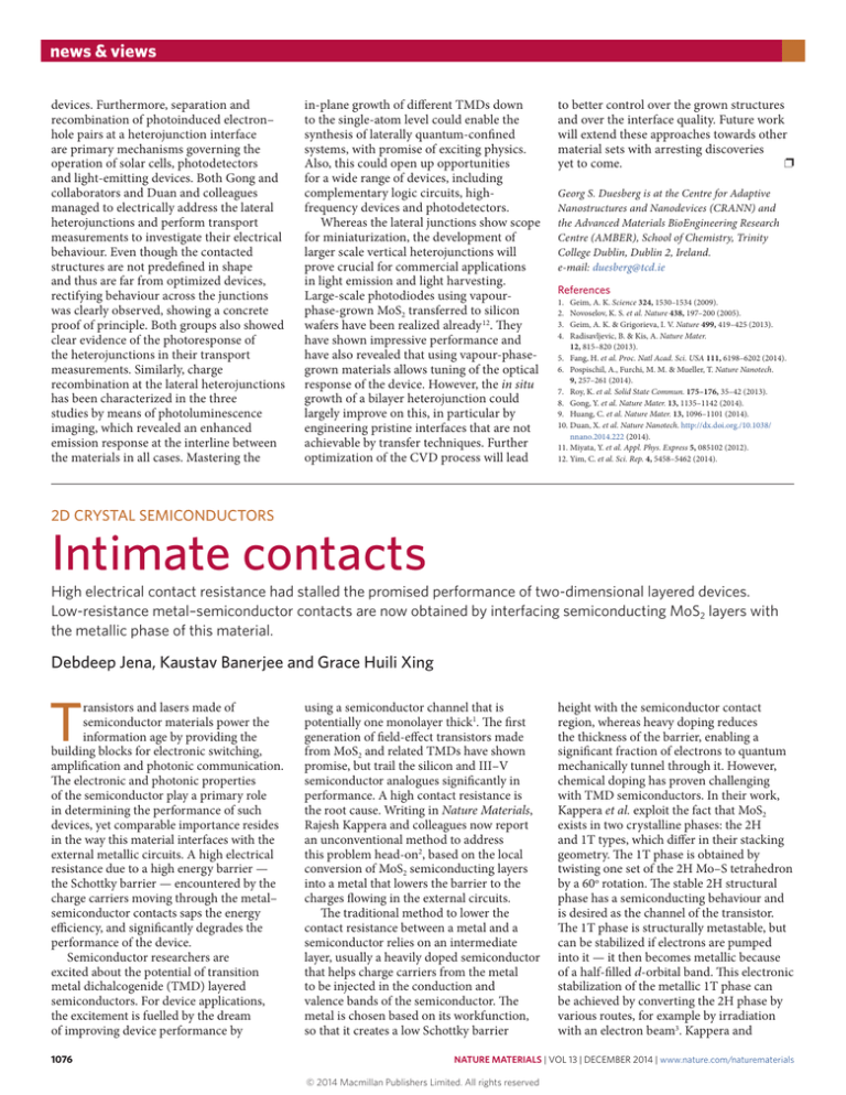
RcW ~h/2e2kF ~0.026/√n 2D kΩ μm, which
NATURE MATERIALS | VOL 13 | DECEMBER 2014 | www.nature.com/naturematerials
© 2014 Macmillan Publishers Limited. All rights reserved
depends strongly on the electron sheet
density (in units of 1013 cm–2) in the
semiconductor channel, and weakly on
some aspects of the bandstructure7. This is
the quantum limit of the contact resistance
for crystalline semiconductors, shown by the
dashed line in Fig. 1.
This limit has been experimentally
verified in atomic break-junctions and in
split-gate quantum point contacts, in which
a quantized conductance was observed8.
The highest-performance semiconductor
transistors are also grazing this lower limit 9,
as shown in Fig. 1. The latest achievements
for TMDs represent a major leap, yet there
is still room for improvement. Recently, a
joint academic and industry research team
has reported a method to chemically dope
MoS2 and have achieved low-resistance
contacts and high-performance transistors10.
Their technique is similar to the traditional
method used for semiconductors, and the
contact resistance values are similar to the
1T contacts discussed here. Both these old
and new approaches mark important steps
towards harnessing the innate potential
of 2D crystal semiconductors. More
importantly, metal–semiconductor junctions
can enable a host of unanticipated physical
phenomena exploiting the d-orbital pedigree
of conduction electrons in TMDs. ❐
Depdeep Jena and Grace Huili Xing are in the
Department of Electrical Engineering, University
of Notre Dame, Indiana 46556, USA, and in
1077
news & views
the Department of Electrical and Computer
Engineering, and Department of Materials Science
& Engineering, Cornell University, New York 14853,
USA. Kaustav Banerjee is in the Department of
Electrical and Computer Engineering, University of
California, Santa Barbara, California 93106, USA.
e-mail: djena@nd.edu
References
1. Radisavlejevic, B., Radenovic, A., Brivio, J., Giacometti, V. &
Kis, A. Nature Nanotech. 6, 147–150 (2011).
2. Kappera, R. et al. Nature Mater. 13, 1128–1134 (2014).
3. Lin, Y.‑C., Dumnenco, D. O., Huang, Y.‑S. & Suenaga, K.
Nature Nanotech. 9, 391–396 (2014).
4. Maxwell, J. C. A Treatise on Electricity and Magnetism
(Clarendon, 1904).
5. Landauer, R. IBM J. Res. Dev. 1, 223–231 (1957).
6. Sharvin, Y. V. Sov. Phys. JETP 21, 655–656 (1965).
7. Datta, S., Assad, F. & Lundstrom, M. S. Superlattices Microstructures
23, 771–780 (1998).
8. Van Wees, B. et al. Phys. Rev. Lett. 60, 848–850 (1988).
9. Maassen, J., Jeong, C., Baraskar, A., Rodwell, M. & Lundstrom, M.
Appl. Phys. Lett. 102, 111605 (2013).
10.Yang, L. et al. VLSI Technol. Digest of Tech. Papers, 2014
Symposium on, 238–239 (2014); http:dx.doi.org/10.1109/
VLSIT.2014.6894432
BIOMINERALIZATION
Crystals competing for space
Analysis of the growth patterns of calcitic prisms within the shell of the fan mollusc Pinna nobilis shows that growth
can be predicted using grain theory and that the organic casings of the prisms set the thermodynamic boundaries.
Nico A. J. M. Sommerdijk and Maggie Cusack
B
iominerals, such as bone, teeth and
shells, are organic–inorganic composite
materials with often amazingly
complex shapes and structures. Biology
uses a variety of minerals to form these
structures — most commonly, calcium
carbonate (CaCO3) and calcium phosphate,
which are used by marine invertebrates
and vertebrates, respectively, as well as iron
oxides and silica1. Growth of biominerals is
thought to be controlled by their interaction
with a complex organic macromolecular
matrix that consists of a specialized
dynamic assembly of (glyco)proteins and
carbohydrate polymers. As a consequence
of these interactions, a high level of
control is achieved over the composition,
a
structure, size and morphology of the
resulting material2. Moreover, through these
interactions the structure and properties
of the biological hybrids are precisely
tuned towards their specific functions: for
example, navigation, mechanical support,
photonics and protection against predation,
often producing physical structures that
surpass those of synthetic analogues.
However, the extent to which the growth
of biominerals is controlled by their
interaction with these organic matrices,
and whether there is also control through
classical thermodynamic parameters,
remains unclear.
Writing in Nature Materials, Zlotnikov
and colleagues now shed light on the shape
b
Figure 1 | Secondary electron images of the calcite prisms and organic casings of the shell of the fan
mollusc, Atrina vexillum. a, Fracture section of the shell of A. vexillum showing the oriented calcite crystals
in the prismatic layer of the shell. Scale bar, 250 μm. b, The organic casings in which the prisms grow.
The prisms were dissolved by incubation in acetic acid (1 M) for 24 h. Scale bar, 50 μm. Images courtesy
of Peter Chung (a,b) and Maggie Cusack (b), University of Glasgow.
1078
evolution of calcite prisms in a mollusc,
and show that the prismatic structure
and morphology can be predicted by
classical thermodynamic theories3. Using
synchrotron-based microtomography, they
analyse the mesostructure of the prisms
forming the calcitic outer layer of the giant
Mediterranean fan mollusc Pinna nobilis
and conclude that only a minimal amount
of biological control is used to create the
well-organized prismatic crystals. Indeed,
other than setting the boundary conditions
of the thermodynamics involved in the
process, the findings of Zlotnikov and
colleagues suggest that the biological
organism has little involvement in the
formation of the finer structural detail of the
outer layer of its shell.
Biomineralization has intrigued
scientists for many decades and serves as
a constant source of inspiration for the
development of new materials with highly
controllable and specialized properties4.
Also, because biological materials are
normally synthesized in aqueous media
and at ambient temperatures — conditions
that are prerequisites for the synthesis of
green materials — a richer understanding
of the biomineralization process may open
new sustainable pathways to materials
with advanced functional and structural
properties. Moreover, the findings reported
by Zlotnikov and colleagues point towards
the simpler nature of the factors that
control this particular biomineralization
process, and if similar strategies could
be exploited by synthetic chemists the
accessibility of green synthesis routes could
be greatly improved.
As a result of their abundance in
nature, biological materials composed of
CaCO3, for example mollusc shells, are the
NATURE MATERIALS | VOL 13 | DECEMBER 2014 | www.nature.com/naturematerials
© 2014 Macmillan Publishers Limited. All rights reserved


