A 0.7 V-to-1.0 V 10.1 dBm-to-13.2 dBm 60
advertisement

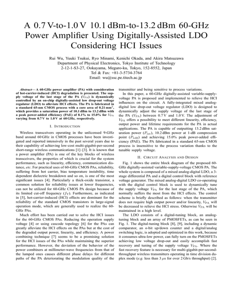
A 0.7 V-to-1.0 V 10.1 dBm-to-13.2 dBm 60-GHz Power Amplifier Using Digitally-Assisted LDO Considering HCI Issues Rui Wu, Yuuki Tsukui, Ryo Minami, Kenichi Okada, and Akira Matsuzawa Department of Physical Electronics, Tokyo Institute of Technology 2-12-1-S3-27, Ookayama, Meguro-ku, Tokyo, 152-8552, Japan Tel & Fax: +81-3-5734-3764 Email: wu@ssc.pe.titech.ac.jp Abstract— A 60-GHz power amplifier (PA) with consideration of hot-carrier-induced (HCI) degradation is presented. The supply voltage of the last stage of the PA (VPA ) is dynamically controlled by an on-chip digitally-assisted low drop-out voltage regulator (LDO) to alleviate HCI effects. The PA is fabricated in a standard 65-nm CMOS process with a core area of 0.21 mm2 , which provides a saturation power of 10.1 dBm to 13.2 dBm with a peak power-added efficiency (PAE) of 8.1% to 15.0% for VPA varying from 0.7 V to 1.0 V at 60 GHz, respectively. I. I NTRODUCTION Wireless transceivers operating in the unlicensed 9-GHz band around 60 GHz in CMOS processes have been investigated and reported intensively in the past several years due to their capability of achieving low-cost multi-gigabit-per-second short-range wireless communications [1]–[3]. It is known that a power amplifier (PA) is one of the key blocks of wireless transceivers, the properties of which is crucial for the system performance, such as linearity, efficiency, communication distance, etc. For practical uses of 60-GHz CMOS PAs, reliability, suffering from hot carrier, bias temperature instability, time dependent dielectric breakdown and so on, is one of the most significant issues [4]. Particularly a thick-oxide transistor, a common solution for reliability issues at lower frequencies, can not be utilized for 60-GHz CMOS PA design because of its limited cut-off frequency (fT ). Furthermore, as indicated in [5], hot-carrier-induced (HCI) effects are dominant for the reliability of the standard CMOS transistors in large-signal operation mode, which are generally used to realize the 60GHz PAs. Much effort has been carried out to solve the HCI issues for the 60-GHz CMOS PAs. Reducing the operation supply voltage [4] or using cascode topology [6] for the PAs can greatly alleviate the HCI effects on the PAs but at the cost of the degraded output power, linearity, and efficiency. A power combining technique [7] seems to be a promising solution for the HCI issues of the PAs while maintaining the superior performance. However, the deviation of the behavior of the power combiners at millimeter-wave frequencies from that of the lumped ones causes different phase delays for different paths of the PA deteriorating the modulation quality of the transmitter and being sensitive to process variations. In this paper, a 60-GHz digitally-assisted variable-supplyvoltage PA is proposed and implemented to relieve the HCI influences on the circuit. A fully-integrated mixed analogdigital low drop-out voltage regulator (LDO) is designed to dynamically adjust the supply voltage of the last stage of the PA (VPA ) between 0.7 V and 1.0 V. The adjustment of VPA offers a possibility to meet different linearity, efficiency, output power and lifetime requirements for the PA in actual applications. The PA is capable of outputting 13.2 dBm saturation power (Psat ), 10.2 dBm power at 1-dB compression point (P1dB ) and achieving 15.0% peak power-added efficiency (PAE). The PA fabricated in a standard 65-nm CMOS process is insensitive to the process variation thanks to the tunable supply voltage. II. C IRCUIT A NALYSIS AND D ESIGN Fig. 1 shows the entire block diagram of the proposed 60GHz digitally-assisted variable-supply-voltage CMOS PA. The whole system is composed of a mixed analog-digital LDO, a 3stage differential PA and a digital control block with reference voltage generator. The mixed analog-digital LDO co-operating with the digital control block is used to dynamically tune the supply voltage VPA for the last stage of the PA, which normally suffers the most from the HCI effects. The control scheme is briefly described as follows: when the transmitter does not require high output power and/or linearity, VPA will be decreased to relieve the HCI stress. Otherwise VPA will be maintained in a high level. The LDO consists of a digital-tuning block, an analogtuning block and an array of PMOSFETs, as can be seen in Fig. 1. The digital-tuning block [8], [9], including a dynamic comparator, an n-bit up/down counter and a digital/analog switching logic, is adopted and optimized in this work, because it consumes ultra-low power, can fully turn on the PMOSFETs achieving low voltage drop-out and easily accomplish fast recovery and tuning of the supply voltage VPA . Where the fast recovery feature is necessary for multi-gigabit-per-secondthroughput wireless transmitters operating in time division duplex mode (e.g. less than 3 µs for over 2 Gb/s throughput) [2]. Digital Control䇭& Reference Voltage Generator This work COMP n-bit up/down counter Digital/Analog switching logic V㫉㪼㪽㪛 Vddin M1 M2 Mn MA Rfb Cfb Vref OpAmp R2 R1 Digital Tuning Analog Tuning C1 PA1 RFin CL VPA PA2 PA3 RFout Fig. 1. System block diagram of the proposed 60-GHz digitally-assisted PA. VPA βVref VrefD Restore Record βV㵭ref Record V㵭refD Restore III. M EASUREMENT R ESULTS Time Training Fig. 2. RFin+ RFin- Awaking Sleep Awaking The transient operation of the mixed analog-digital LDO. MIM TL TL M1 Vdd Vg2 Cc2 Cc1 Cc2 M4 Fig. 3. M3 M2 Vg1 Cc1 M5 from minimum to maximum value by adjusting the reference voltage of the digital-tuning block (VrefD ). The digital control bits of the PMOSFETs (M1 to Mn ) for different values of VrefD are recorded to the digital control block. Once the training period is finished, when the value of VPA is larger than the setting value of VrefD , the LDO is switched from digital to analog mode by the switching logic. After a period of charging (or discharging), the LDO outputs a constant VPA at the value of βVref , where β = (R1 + R2 )/R2 and Vref is the reference voltage of the analog-tuning block, as depicted in Fig. 2. When the desired value of VPA is changed or/and the circuit is awakened from sleep mode, the digital control block restores the control bits for M1 to Mn to the up/down counter and generates reference voltages correspondingly. VPA will be instantly charged (or discharged) to the value corresponding to the restored digital control bits, then tuned by the analog block of the LDO to the desired value in a short time. Simulation results show that the recovery time of VPA is less than 0.1 µs. The schematic of the 3-stage differential CMOS PA is shown in Fig. 3. The HCI effects on the PA are further alleviated owing to the adoption of the differential topology. A transmission line (TL) with 0.8 dB/mm loss around 60 GHz is used for matching network, and an MIM transmission line (MIM TL) is realized for the de-coupling of the power supplies. The stability and power gain of the PA are improved by incorporating the capacitive cross-coupling technique for the first and second stages of the PA [10], [11]. Vdd Vg3 M6 RFout- VPA RFout+ The 3-stage differential PA core. The analog-tuning block is utilized to avoid the inherently large ripple of the digital-tuning block when the 3-stage PA is working. Fig. 2 illustrates the transient operation of the mixed analog-digital LDO with the assistance of the digital control block for fast tuning and recovery of the supply voltage VPA . At the beginning of the LDO operation, the digitaltuning block goes through a training period while analogtuning block is turned off by the switching logic. VPA is swept To verify our design, the core blocks of the proposed 60GHz PA including the mixed analog-digital LDO and the 3-stage differential PA are fabricated in a standard 65 nm CMOS technology. Fig. 4 shows the die micro-photograph of the circuit. The areas of the 3-stage differential PA and the mixed analog-digital LDO are 0.132 mm2 and 0.025 mm2 , respectively. The on-chip de-coupling capacitor (CL ) is 86 pF with a size of 0.051 mm2 . The supply voltage of the first and second stages of the PA (Vdd ) and the external input voltage of the LDO (Vddin ) are set to be 1.2 V for demonstration simplicity. As depicted in Fig. 5, the small-signal S-parameters of the PA is measured for different values of VPA . The 3dB bandwidth is about 13 GHz (from 53 GHz to 66 GHz) for all the measurement values of VPA . The peak gain is 19.7 dB and 17.0 dB at 59 GHz for VPA = 1.0 V and VPA = 0.7 V, respectively. The measured Psat , P1dB and maximum PAE (PAEmax ) are plotted versus VPA at 60 GHz in Fig. 6. The P1dB is reduced from 10.2 dBm to 5.8 dBm when VPA is tuned from 1.0 V to 0.7 V as can be observed in Fig. 6. The HCI stress on the circuit is therefore lightened by decreasing the supply voltage and output power simultaneously, which leads to a better lifetime for the proposed PA. In Fig. 7, the experimental lifetime of the NMOSFETs used in the last stage of the PA is illustrated under different stress conditions. The lifetime is defined as the time when the drain current 15 LDO Psat Psat and P1dB (dBm) 12 PA 25 P1dB 9 20 6 15 3 PAEmax (%) CL 30 10 PAEmax 0 Die micro-photograph. Chip size: 0.70×0.80 mm2 including pads. Fig. 4. 5 0.7 0.8 0.9 1.0 VPA (V) 25 Fig. 6. 100 Lifetime (year) 20 Sdd21 (dB) Measured Psat , P1dB and PAEmax versus VPA at 60 GHz. 15 10 VPA = 0.7 V VPA = 0.8 V VPA = 1.00 V 10 VPA = 0.75 V 1 VPA = 1.0 V 5 0.1 0 47 Fig. 5. 52 57 Freq. (GHz) 62 67 Measured Sdd21 for various values of VPA . of the transistor (IDS ) decreases by 10% from the unstressed value. When the output power of the PA (Pout ) is 10 dBm and VPA = 1.0 V, the lifetime of the NMOSFETs is only 0.2 year. While if Pout = 5 dBm and VPA = 0.75 V, the lifetime is improved to about 30 years. Table I summarizes and compares the performance of the proposed power amplifier with that of the state-of-the-art PAs at 60 GHz in CMOS processes. It is shown in table I that the proposed PA exhibits comparable output power and efficiency at high supply voltage (VPA = 1.0 V) to the recently published PAs in the 60-GHz band for CMOS technologies. Meanwhile, at low supply voltage (VPA = 0.7 V), the proposed PA with reasonable output power, efficiency and linearity still can be used for shorter distance communications or/and low-level modulation schemes (e.g. BPSK and QPSK). As demonstrated in Fig. 8, the measured output spectrum of the proposed PA barely degrades when VPA is reduced from 1.0 V to 0.7 V and output power is comparable. The measurement is performed by applying a QPSK modulation signal to the input of the PA at channel 3 (61.56 GHz to 63.72 GHz ) of IEEE 802.15.3c with a symbol rate of 1.76 Gs/s. The center frequency of this channel is 62.64 GHz. Both of the spectrums meet the IEEE 802.15.3c standard. Fig. 9 shows the measured EVM 2 4 6 8 Pout (dBm) 10 12 Fig. 7. Experimental lifetime of the NMOSFETs for different values of output power Pout and VPA . at various values of VPA and Pout . The channel 3 of IEEE 802.15.3c and 3.52-Gb/s QPSK modulation signal are chosen again to evaluate the EVM performance of the proposed PA. All the measured EVM is lower than -17 dB and satisfies IEEE 802.15.3c standard. It can be observed that the measured EVM is from 11.7% (-18.6 dB) to 12.9% (-17.8 dB) for low output power (Pout = 5 dBm) if VPA is tuned from 1.0 V to 0.7 V. The degradation of the EVM is less than 1 dB, which implies the low supply voltage VPA is preferred for low output power situation considering the HCI issues. While at high output power (Pout = 10 dBm), the measurement value of the EVM is 13.1% (-17.7 dB) and 13.6% (-17.3 dB) for VPA = 1.0 V and VPA = 0.9 V, respectively. IV. C ONCLUSION This paper presents a 60-GHz variable-supply-voltage power amplifier using the digitally-assisted LDO in a 65-nm CMOS process. The severe HCI issues for 60-GHz CMOS power amplifiers have been greatly alleviated at low supply voltage (VPA = 0.7 V). The lifetime of the proposed PA can be improved to over 30 years. On the other hand, the power amplifier is still able to provide 13.2 dBm saturation power, 10.2 dBm power at 1-dB compression point and 15.0% TABLE I 60-GH Z CMOS PA P ERFORMANCE C OMPARISON . Ref. CMOS Process Freq. (GHz) [4] 90 nm 60 [6] 65 nm SOI 60 [7] [11] 65 nm 65 nm 60 60 This work 65 nm 60 * Supply (V) Psat (dBm) P1dB (dBm) PAEmax (%) 0.7 1.0 1.2 1.8 2.6 1.0 1.0 8.5 11.5 10.5 14.5 16.5 18.6 11.5 10.1 13.2 5.2 8.0 7.1 12.7 15.2 15.0 8.0 5.8 10.2 7.0 15.2 22.3 25.7 18.2 15.1 15.2 8.1 15.0 0.7* 1.0* IEEE 802.15.3c Spectrum mask 0.573 0.28 0.696 0.56 R EFERENCES Magnitude (dB) 0 -10 -20 -30 -40 -50 -10 -20 -30 -40 -50 -2.5 -1.5 -0.5 0.5 1.5 2.5 Normalized Freq. (GHz) (a) -2.5 -1.5 -0.5 0.5 1.5 2.5 Normalized Freq. (GHz) (b) Fig. 8. Measured output spectrum of the proposed PA normalized to 62.64 GHz for QPSK modulation (a) VPA = 1.0 V, Pout = 4 dBm; (b) VPA = 0.7 V, Pout = 3 dBm. -15 Pout = 5 dBm Pout = 7 dBm -16 Pout = 10 dBm EVM (dB) 0.18 (core) Only for the last stage VPA 0 Magnitude (dB) Area (mm2 ) -17 -18 -19 -20 0.7 0.8 0.9 1 VPA (V) Fig. 9. Measured EVM versus VPA for QPSK modulation at different output power level. peak power-added efficiency at 60 GHz for high supply voltage (VPA = 1.0 V). The performance of the proposed PA at various VPA conditions meets the requirements of short-range multi-gigabit-per-second communication standards (e.g. IEEE 802.15.3c). ACKNOWLEDGMENT This work was partially supported by MIC, SCOPE, MEXT, STARC, NEDO, Canon Foundation, and VDEC in collaboration with Cadence Design Systems, Inc., and Agilent Technologies Japan, Ltd. [1] K. Okada, K. Kondou, M. Miyahara, M. Shinagawa, H. Asada, R. Minami, T. Yamaguchi, A. Musa, Y. Tsukui, Y. Asakura, S. Tamonoki, H. Yamagishi, Y. Hino, T. Sato, H. Sakaguchi, N. Shimasaki, T. Ito, Y. Takeuchi, N. Li, Q. Bu, R. Murakami, K. Bunsen, K. Matsushita, M. Noda, and A. Matsuzawa, “A full 4-channel 6.3 Gb/s 60 GHz directconversion transceiver with low-power analog and digital baseband circuitry,” in IEEE ISSCC Dig. Tech. Papers, 2012, pp. 218–219. [2] T. Mitomo, Y. Tsutsumi, H. Hoshino, M. Hosoya, T. Wang, Y. Tsubouchi, R. Tachibana, A. Sai, Y. Kobayashi, D. Kurose, T. Ito, K. Ban, T. Tandai, and T. Tomizawa, “A 2 Gb/s-throughput CMOS transceiver chipset with in-package antenna for 60 GHz short-range wireless communication,” in IEEE ISSCC Dig. Tech. Papers, 2012, pp. 266–267. [3] V. Vidojkovic, G. Mangraviti, K. Khalaf, V. Szortyka, K. Vaesen, W. V. Thillo, B. Parvais, M. Libois, S. Thijs, J. R. Long, C. Soens, and P. Wambacq, “A low-power 57-to-66 GHz transceiver in 40 nm LP CMOS with -17 dB EVM at 7 Gb/s,” in IEEE ISSCC Dig. Tech. Papers, 2012, pp. 268–269. [4] M. Tanomura, Y. Hamada, S. Kishimoto, M. Ito, N. Orihashi, K. Maruhashi, and H. Shimawaki, “TX and RX front-ends for 60 GHz band in 90 nm standard bulk CMOS,” in IEEE ISSCC Dig. Tech. Papers, 2008, pp. 558–559. [5] L. Negre, D. Roy, F. Cacho, P. Scheer, S. Jan, S. Boret, D. Gloria, and G. Ghibaudo, “Reliability characterization and modeling solution to predict aging of 40-nm MOSFET DC and RF performances induced by RF stress,” IEEE J. Solid-State Circuits, vol. 47, no. 5, pp. 1075–1083, May 2012. [6] A. Siligaris, Y. Hamada, C. Mounet, C. Raynaud, B. Martineau, N. Deparis, N. Rolland, M. Fukaishi, and P. Vincent, “A 60 GHz power amplifier with 14.5 dBm saturation power and 25% peak PAE in CMOS 65 nm SOI,” IEEE J. Solid-State Circuits, vol. 45, no. 7, pp. 1286–1294, Jul. 2010. [7] J. Chen and A. M. Niknejad, “A compact 1 V 18.6 dBm 60 GHz power amplifier in 65 nm CMOS,” in IEEE ISSCC Dig. Tech. Papers, 2011, pp. 432–433. [8] Y. Okuma, K. Ishida, Y. Ryu, X. Zhang, P.-H. Chen, K. Watanabe, M. Takamiya, and T. Sakurai, “0.5-V input digital LDO with 98.7% current efficiency and 2.7-mA quiescent current in 65 nm CMOS,” in Proc. IEEE CICC, 2010, pp. 323–326. [9] K. Hirairi, Y. Okuma, H. Fuketa, T. Yasufuku, M. Takamiya, M. Nomura, H. Shinohara, and T. Sakurai, “13% power reduction in 16 b integer unit in 40 nm CMOS by adaptive power supply voltage control with paritybased error prediction and detection (PEPD) and fully integrated digital LDO,” in IEEE ISSCC Dig. Tech. Papers, 2012, pp. 486–487. [10] H. Asada, K. Bunsen, K. Matsushita, R. Murakami, Q. Bu, A. Musa, T. Sato, T. Yamaguchi, R. Minami, T. Ito, K. Okada, and A. Matsuzawa, “A 60 GHz 16 Gb/s 16QAM low-power direct-conversion transceiver using capacitive cross-coupling neutralization in 65 nm CMOS,” in Proc. IEEE A-SSCC, 2011, pp. 373–376. [11] W. L. Chan and J. R. Long, “A 58–65 GHz neutralized CMOS power amplifier with PAE above 10% at 1-V supply,” IEEE J. Solid-State Circuits, vol. 45, no. 3, pp. 554–564, Mar. 2010.


