LETTERS
PUBLISHED ONLINE: 24 NOVEMBER 2013 | DOI: 10.1038/NPHOTON.2013.311
Photocurrent generation in semiconducting and
metallic carbon nanotubes
Maria Barkelid* and Val Zwiller
The fundamental mechanism underlying photocurrent generation in carbon nanotubes1–3 has long been an open question.
In photocurrent generation, the temperature of the photoexcited charge carriers determines the transport regime by
which the electrons and holes are conducted through the nanotube. Here, we identify two different photocurrent mechanisms
for metallic and semiconducting carbon nanotube devices with
induced p–n junctions4–7. Our photocurrent measurements as a
function of charge carrier doping demonstrate a thermal
origin8,9 for metallic nanotubes, where photo-excited hot
carriers give rise to a current. For semiconducting nanotubes
we demonstrate a photovoltaic mechanism10–12, where a builtin electric field results in electron–hole separation. Our
results provide an understanding of the photoresponse in
carbon nanotubes, which is not only of fundamental interest
but also of importance for designing carbon-based, highefficiency photodetectors and energy-harvesting devices.
To develop sophisticated photonic devices13–15, the physical processes governing the electro-optical response must be understood.
The process of photocurrent generation has been widely studied
in both supported4,5 and suspended6,7 carbon nanotubes, but its
origin remains controversial. Two mechanisms compete in carbon
nanotubes, the photovoltaic effect10–12, where photocurrent arises
from an electric field, and the photothermal effect8,9, where the
photocurrent results from a difference in Seebeck coefficients.
Recent studies have established a fingerprint technique for distinguishing between the photothermal and photovoltaic effects in
graphene16–18. This technique assigns a six-fold-symmetric pattern
in the doping-dependent photocurrent response to the photothermoelectric effect and a two-fold symmetry to the photovoltaic
effect. Here, we perform doping-dependent photocurrent measurements on individually suspended carbon nanotube devices to
investigate the generation of photocurrent.
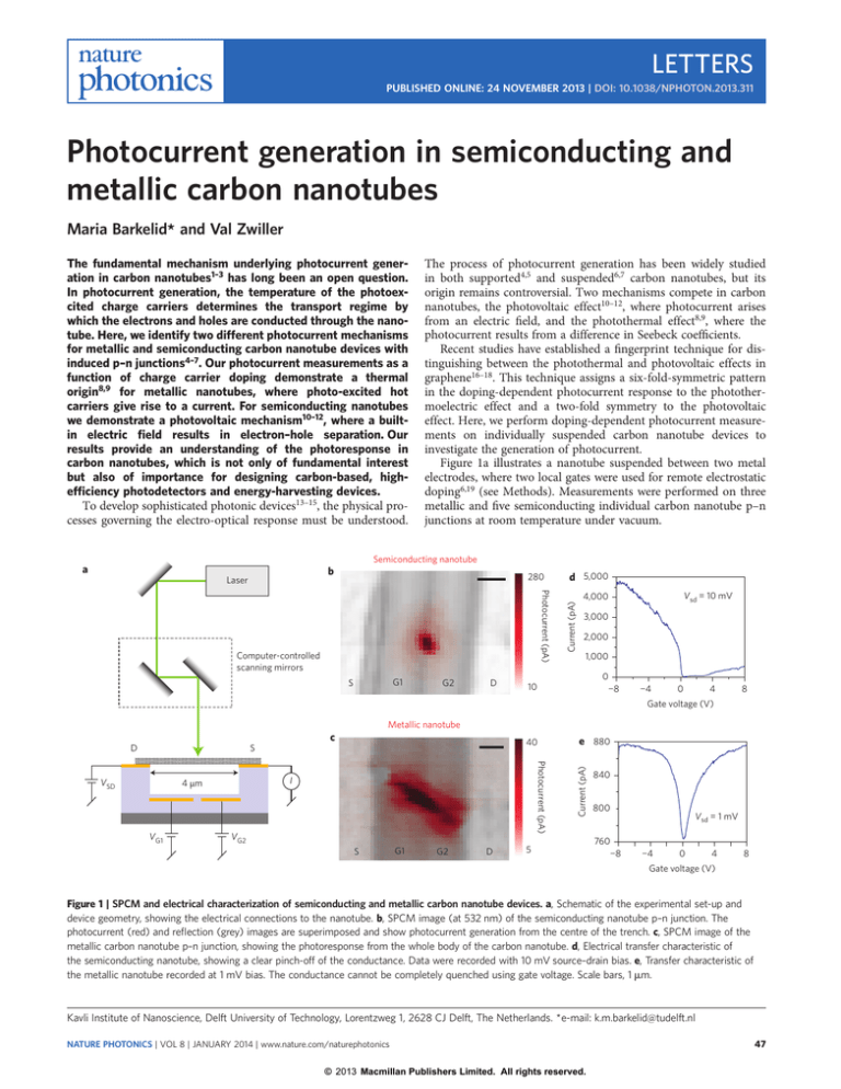
Figure 1a illustrates a nanotube suspended between two metal
electrodes, where two local gates were used for remote electrostatic
doping6,19 (see Methods). Measurements were performed on three
metallic and five semiconducting individual carbon nanotube p–n
junctions at room temperature under vacuum.
Semiconducting nanotube
b
Laser
280
Photocurrent (pA)
Computer-controlled
scanning mirrors
G1
S
G2
D
d 5,000
Current (pA)
a
Vsd = 10 mV
4,000
3,000
2,000
1,000
0
−8
10
−4
0
4
8
Gate voltage (V)
Metallic nanotube
S
D
I
4 μm
VG1
Photocurrent (pA)
VSD
40
VG2
S
G1
G2
D
e 880
Current (pA)
c
5
840
800
760
−8
Vsd = 1 mV
−4
0
4
8
Gate voltage (V)
Figure 1 | SPCM and electrical characterization of semiconducting and metallic carbon nanotube devices. a, Schematic of the experimental set-up and
device geometry, showing the electrical connections to the nanotube. b, SPCM image (at 532 nm) of the semiconducting nanotube p–n junction. The
photocurrent (red) and reflection (grey) images are superimposed and show photocurrent generation from the centre of the trench. c, SPCM image of the
metallic carbon nanotube p–n junction, showing the photoresponse from the whole body of the carbon nanotube. d, Electrical transfer characteristic of
the semiconducting nanotube, showing a clear pinch-off of the conductance. Data were recorded with 10 mV source–drain bias. e, Transfer characteristic of
the metallic nanotube recorded at 1 mV bias. The conductance cannot be completely quenched using gate voltage. Scale bars, 1 mm.
Kavli Institute of Nanoscience, Delft University of Technology, Lorentzweg 1, 2628 CJ Delft, The Netherlands. * e-mail: k.m.barkelid@tudelft.nl
NATURE PHOTONICS | VOL 8 | JANUARY 2014 | www.nature.com/naturephotonics
© 2013 Macmillan Publishers Limited. All rights reserved.
47
LETTERS
NATURE PHOTONICS
a
Metallic nanotube
−120
Photocurrent (pA)
50
Semiconducting nanotube
c
Photocurrent (pA)
−20
250
8
15
8
nn
pp
pn
np
nn
pp
pn
Gate 1 ( V)
Gate 1 ( V)
np
−8
−8
−8
−8
8
Gate 2 (V)
8
Gate 2 (V)
d
Photocurrent (pA)
b
Photocurrent (pA)
DOI: 10.1038/NPHOTON.2013.311
100
0
−100
−8
e
8
Gate 2 (V)
1.2
Resistance (MΩ)
1.4
−10
−20
−8
8
Gate 2 (V)
100
f
8
Resistance (MΩ)
500
8
np
nn
pp
pn
np
nn
pp
pn
Gate 1 ( V)
Gate 1 (V)
−8
−8
0
Gate 2 (V)
8
−8
−8
Gate 2 (V)
8
Figure 2 | Gate-dependent conductivity. a, Photocurrent map of a metallic nanotube, displaying a six-fold pattern characteristic of the photothermal effect.
b, Line profile of the photocurrent along the yellow line in a, showing the multiple sign changes of the photocurrent as a function of gate voltage.
c, Photocurrent map of a semiconducting nanotube, displaying a two-fold pattern characteristic of the photovoltaic effect. d, Line profile of the photocurrent
along the yellow line in c, clearly showing a single sign change of the photocurrent as a function of gate voltage. e, Resistance as a function of gate voltage
for the metallic nanotube. The high-resistance ridges agree with the vertical and horizontal sign changes in the photocurrent map in a. f, Resistance map for
the semiconducting nanotube. The transition between high- and low-conductance regions corresponds to the transitions in the photocurrent map in c.
Scanning photocurrent microscopy (SPCM)4,10,11 images of
semiconducting and metallic nanotube p–n junctions (gate
voltage, +8 V), with zero source–drain bias, were obtained with a
532 nm (1.45 kW cm22) laser. The photocurrent and reflection
images were superimposed, generating Fig. 1b and c. The semiconducting nanotube in Fig. 1b shows photocurrent generated at the
p–n junction formed between the two gates. The photocurrent
from the metallic nanotube p–n junction in Fig. 1c has a much
broader distribution, possibly a result of inefficient coupling to
phonons20, resulting in a thermal gradient extending along the
nanotube due to the long electron cooling length21.
The transfer characteristics of the two nanotubes are shown in
Fig. 1d,e. With a bias of 10 mV across the semiconducting nanotube,
48
both gate voltages were swept from negative to positive values. The
electron conductance is 10 times lower than the hole conductance
due to a poor n-type contact. In the metallic nanotube, with a
bias of 1 mV, the conductance could be modulated by the gate
voltage, but could not be quenched.
After spatial imaging, the laser was targeted at the p–n junction
and the photoresponse was recorded as a function of gate voltage
(l ¼ 532 nm, P ¼ 1.45 (2.9) kW cm22 for the semiconducting
(metallic) nanotube). The metallic nanotube in Fig. 2a shows a
clear six-fold pattern, characteristic of the photothermal effect. As
predicted and demonstrated for graphene16,17, this characteristic
pattern arises from the dependence of the photocurrent on the
Seebeck coefficient S. In agreement with ref. 16, due to the close
NATURE PHOTONICS | VOL 8 | JANUARY 2014 | www.nature.com/naturephotonics
© 2013 Macmillan Publishers Limited. All rights reserved.
NATURE PHOTONICS
a
LETTERS
DOI: 10.1038/NPHOTON.2013.311
S
Nanotube
D
−50
b
Semiconducting nanotube
Photocurrent (pA)
50
10
Photocurrent (pA)
−8
pp
60
40
Gate 1 and 2 (V)
c
Photocurrent (pA)
−40
20
0
−20
−40
nn
−60
−8
−4
0
4
8
8
S
Gate voltage (V)
e
Metallic nanotube
S
Photocurrent (pA)
−15
f 120
Photocurrent (pA)
Photocurrent (pA)
100
15
D
Nanotube
−50
80
−8
pp
Gate 1 and 2 (V)
d
D
Nanotube
40
0
−40
nn
−80
8
−8
−4
0
4
8
S
Gate voltage (V)
Nanotube
D
Figure 3 | Photocurrent response for homogeneous doping. a, SPCM image of the semiconducting nanotube with homogeneous p-doping. b, The laser is
scanned along the nanotube axis (yellow line in a) while changing the doping from p-type to n-type. The photocurrent response shifts towards the centre of
the nanotube for low doping levels. c, Line profile along the left green line in b. The photocurrent increases with gate voltage, resulting from the sign change
of the electric field at the Schottky barrier. d, SPCM image of the metallic nanotube with p-doping. e, The laser is scanned along the yellow line in d, while
tuning the gate voltage. The photocurrent from the nanotube–electrode interface shows no spatial shift with gate voltage. f, Line profile along the left
green line in e. The photocurrent shows a non-monotonic trend originating from the Seebeck effect. Measurements were performed at 532 nm. All scale
bars, 1 mm.
dependence on chemical potential the Seebeck coefficient has a
non-monotonic dependence on gate voltage16,22. This results in
several polarity reversals of (Sregion2 2 Sregion1). The photothermal
current in the metallic nanotube arises from this difference in
Seebeck coefficient in the two regions of the nanotube and hence
displays multiple sign changes, giving rise to the six distinct
regions in Fig. 2a. A line profile is presented in Fig. 2b, which
demonstrates the multiple sign changes in the photocurrent. The
thermally excited hot carriers decay through carrier multiplication
into several low-energy electrons, leading to a local hot carrier
distribution23,24.
A photocurrent map was also recorded for the semiconducting
nanotube (Fig. 2c), which displays a characteristic two-fold
pattern indicative of the photovoltaic effect, where the direction of
the photocurrent is parallel to the built-in electric field at the junction. An intense photocurrent signal is generated for p–n and n–p
doping due to the presence of the electric field dissociating the excitons. For a homogeneously p-doped or n-doped nanotube the
photocurrent is negligible, as the electric field is not sufficient to separate the exciton into free charge carriers. In the photovoltaic effect,
when tuning the gate voltage, and thereby the charge carrier concentration, the sign of the electric field at the junction changes. For
increasing gate voltage, the electric field only changes sign once,
resulting in a single polarity change of the photocurrent.
Figure 2d presents a line profile of the photocurrent as a function
of gate voltage. The sign changes in the photocurrent map in
NATURE PHOTONICS | VOL 8 | JANUARY 2014 | www.nature.com/naturephotonics
© 2013 Macmillan Publishers Limited. All rights reserved.
49
LETTERS
NATURE PHOTONICS
50
70
Semiconducting
Metallic
60
/4
50
Photocurrent (pA)
Fig. 2c do not occur exactly at zero gate voltage, as a result of the two
trench gates not coupling equally to the nanotube or the semiconducting nanotube being slightly p-doped.
Our key observation from Fig. 2 is the existence of two distinctly
different patterns in the photocurrent response in semiconducting
and metallic nanotubes. This shows that the dominant mechanism
for the generation of photocurrent differs in the two nanotubes.
External factors could potentially suppress the contribution from
one or both mechanisms25,26. Accordingly, we defined a set of experimental conditions that justify a comparison between the metallic
and semiconducting nanotubes (see Methods). All nanotubes
were measured under identical conditions.
We compared the conductivity in the nanotubes with and
without illumination. The resistance measurements in Fig. 2e,f,
were obtained from current measurements with a bias of 1 mV
and 10 mV, respectively. The resistance map of the metallic nanotube shows two highly resistive ridges. This dip in conductivity,
similar to that in Fig. 1e, causes a change in the Seebeck coefficient.
The photocurrent in Fig. 2a arising from the difference in the
Seebeck coefficient displays a polarity change for the same gate voltages. One additional polarity change is seen along the diagonal in
the photocurrent map, which does not have a counterpart in the
resistance map. As the doping level is homogeneous, the Seebeck
coefficient is uniform along the nanotube and cannot provide a
directionality for the thermally excited carriers, and hence makes
no net contribution to the photocurrent.
For a homogeneously doped semiconducting nanotube, high
conductivity is observed (Fig. 2f ), but the photocurrent (Fig. 2c)
is negligible. This is a result of the absence of a local electric field.
For p–n and n–p doping the device exhibits a large resistance as
well as a large photocurrent response due to the presence of an
electric field at the junction.
To support the existence of different photocurrent generation
mechanisms, the photocurrent response along the nanotube axis
was investigated as a function of doping. The device was tuned
from homogeneous p-type to n-type while scanning the laser
along the nanotube axis. The laser path is indicated in Fig. 3a for
p-type doping of the semiconducting nanotube. Figure 3b shows
the photocurrent shifting towards the centre of the nanotube with
decreasing doping11. This arises from a shift in the maximum electric field at the Schottky barriers towards the centre of the nanotube,
resulting from the extension of the depletion region with decreasing
doping concentration27. A line profile of the photocurrent taken
along the left green line in Fig. 3b is presented in Fig. 3c, and
shows a continuous increase in photocurrent with increasing gate
voltage. This is an effect of the electric field at the Schottky
barrier changing sign.
The metallic nanotube (shown with p-type doping in Fig. 3d) has
a much less pronounced shift in the photocurrent response, as can
clearly be seen in Fig. 3e. The photocurrent, originating from the
difference in Seebeck coefficient of the metallic nanotube and
the metal electrode, is generated when the laser is positioned at
the nanotube–electrode interface. We tuned the Seebeck coefficient
of our metallic nanotube with the gate voltage, causing the photocurrent to change sign. Figure 3f presents a line profile (along the
left green line in Fig. 3e), and shows a non-monotonic dependence
on gate voltage, characteristic of the Seebeck effect. The photocurrent responses from the nanotube–electrode interfaces show
behaviour comparable to that of the photocurrent from the p–n
junctions, consistent with our observations of the photothermal
and photovoltaic effects dominating in metallic and semiconducting
nanotubes, respectively.
We next studied the photocurrent profile as a function of position along the nanotube axis. The photocurrent from the semiconducting nanotube p–n junction is shown in Fig. 4 (blue). The
electric field at the junction was probed by the incident laser with
DOI: 10.1038/NPHOTON.2013.311
40
30
20
Contact
Contact
10
0
−10
0
1
2
3
4
5
6
7
Laser spot position (µm)
Figure 4 | Spatial photocurrent response. Photocurrent as a function of
laser spot position for the semiconducting and metallic carbon nanotube
p–n junctions (blue and red, respectively). The photocurrent from the
semiconducting nanotube has been fitted with a Gaussian profile, originating
from the laser spot profile, which is probed by the electric field at the
junction. The photocurrent response from the metallic nanotube follows a
triangular profile, indicating that the charge carriers stay hot until they reach
the contacts, in agreement with the photothermal effect. Measurements
were recorded with a 532 nm laser.
a Gaussian profile, which determines the profile of the photocurrent.
The data were fitted to a Gaussian, and divided by a factor of four for
clarity. The tails come from the laser spot not being perfectly diffraction-limited. The photocurrent from the metallic nanotube p–n
junction is shown in red in Fig. 4. The photocurrent follows a triangular profile, centred at the p–n junction and extending 2 mm
on each side. The broad triangular shape indicates that the photogenerated carriers are hot and follow a thermal distribution
through the nanotube. At the electrode–nanotube interface the
photocurrent changes sign, possibly a result of band bending at
the contacts or a difference in the Seebeck coefficient between the
electrode and the nanotube (see Supplementary Section 3). This
difference in photocurrent features confirms that the photocurrent
in semiconducting nanotubes results from an electric field and in
metallic nanotubes is a thermal effect.
In summary, we have presented clear evidence that different
photocurrent generation mechanisms dominate the photocurrent
response in metallic and semiconducting nanotubes. Metallic
nanotubes exhibit a dominating photothermal effect, whereas the
photovoltaic effect dominates the photocurrent response in semiconducting nanotubes. A detailed understanding of the physical
processes that govern photocurrent generation in carbon nanotubes
is the first important step towards optimizing the design of optoelectronic devices for photodetection and energy harvesting28,29. This
will enable highly efficient optical components based on carbon
nanotubes to be engineered.
Methods
Fabrication. The device geometry was designed to individually suspend the carbon
nanotubes across a trench with metal gates at the bottom of the trench. Beginning
with a piece of silicon wafer covered with 285 nm thermal SiO2 , two trench gates
were patterned using electron-beam lithography followed by evaporation of
5 nm tungsten and 25 nm platinum. The gates were 2 mm wide and separated by
250 nm. Next, 1 mm of SiO2 was deposited using PECVD and the trench was created
by etching away the oxide above the gate region, creating an 800-nm-deep and
4-mm-wide trench. The source and drain electrodes were defined on both sides of
the trench using electron-beam lithography and metal evaporation (5 nm tungsten
and 25 nm platinum). Finally, the FeMo catalyst area was patterned with
electron-beam lithography on top of the metal contact, and the catalyst solution was
NATURE PHOTONICS | VOL 8 | JANUARY 2014 | www.nature.com/naturephotonics
© 2013 Macmillan Publishers Limited. All rights reserved.
NATURE PHOTONICS
LETTERS
DOI: 10.1038/NPHOTON.2013.311
drop-coated onto the sample, followed by lift-off. The carbon nanotubes were
grown30 across the trench, using CH4 and H2 in a CVD oven at 900 8C.
Measurement set-up. The suspended carbon nanotube devices were placed in a
cryostat under vacuum. Characterization was carried out by scanning the laser beam
across a defined area of the sample by means of two computer-controlled scanning
galvo-mirrors. The laser was focused onto the sample with an objective with a
numerical aperture of 0.8. SPCM was performed and the reflected light from the
sample structure was collected by a silicon photodiode. The measurements were
performed at room temperature with a 532 nm continuous-wave laser.
Experimental conditions. In this study we chose a set of experimental conditions so
as to make a fair comparison between semiconducting and metallic carbon
nanotubes. The nanotubes were suspended to avoid heatsinking from the substrate,
which suppresses the photothermal effect. The platinum contact metal was identical
for all devices. To minimize the influence from defects, the nanotubes were grown in
the final fabrication step and were not subjected to any post-growth fabrication.
This resulted in negligible defects being present. The nanotubes were excited
off-resonance. This enabled more comparable measurement conditions, as the
resonances in the metallic nanotubes could not be probed. All measurements were
performed at room temperature.
Received 26 April 2013; accepted 16 October 2013;
published online 24 November 2013
References
1. Biercuk, M. J., Ilani, S., Marcus, C. M. & McEuen, P. L. Electrical transport in
single-walled carbon nanotubes. Top. Appl. Phys. 111, 455–493 (2008).
2. Dresselhaus, M. S., Dresselhaus, G., Charlier, J. C. & Hernandez, E. Electronic,
thermal and mechanical properties of carbon nanotubes. Phil. Trans. R. Soc.
Lond. A 362, 2065–2098 (2004).
3. Dresselhaus, M. S., Dresselhaus, G., Saito, R. & Jorio, A. Exciton photophysics of
carbon nanotubes. Annu. Rev. Phys. Chem. 58, 719–747 (2007).
4. Freitag, M., Martin, Y., Misewich, J. A., Martel, R. & Avouris, P. H.
Photoconductivity of single carbon nanotubes. Nano Lett. 3, 1067–1071 (2003).
5. Gabor, N. M., Zhong, Z., Bosnick, K., Park, J. & McEuen, P. L. Extremely
efficient multiple electron–hole pair generation in carbon nanotube
photodiodes. Science 325, 1367–1371 (2009).
6. Lee, J. U., Gipp, P. P. & Heller, C. M. Carbon nanotube p–n junction diodes.
Appl. Phys. Lett. 85, 145–147 (2004).
7. Barkelid, M., Steele, G. A. & Zwiller, V. Probing optical transitions in individual
carbon nanotubes using polarized photocurrent spectroscopy. Nano Lett. 12,
5649–5653 (2012).
8. St-Antoine, B. C., Menard, D. & Martel, R. Position sensitive
photothermoelectric effect in suspended single-walled carbon nanotube films.
Nano Lett. 9, 3503–3508 (2009).
9. Tsen, A. W., Donev, L. A. K., Kurt, H., Herman, L. H. & Park, J. Imaging the
electrical conductance of individual carbon nanotubes with photothermal
current microscopy. Nature Nanotech. 4, 108–113 (2008).
10. Balasubramanian, K., Burghard, M., Kern, K., Scolari, M. & Mews, A.
Photocurrent imaging of charge transport barriers in carbon nanotube devices.
Nano Lett. 5, 507–510 (2005).
11. Ahn, Y. H., Tsen, A. W., Kim, B., Park, Y. W. & Park, J. Photocurrent imaging of
p–n junctions in ambipolar carbon nanotube transistors. Nano Lett. 7,
3320–3323 (2007).
12. Balasubramanian, K., Fan, Y., Burghard, M. & Kern, K. Photoelectronic
transport imaging of individual semiconducting carbon nanotubes. Appl. Phys.
Lett. 84, 2400 (2004).
13. Mueller, T. et al. Efficient narrow-band light emission from a single carbon
nanotube p–n diode. Nature Nanotech. 5, 27–31 (2010).
14. Barone, P. W., Baik, S., Heller, D. A. & Strano, M. S. Near-infrared optical
sensors based on single-walled carbon nanotubes. Nature Mater. 4,
86–92 (2005).
15. Lee, J. U. Photovoltaic effect in ideal carbon nanotube diodes. Appl. Phys. Lett.
87, 073101 (2005).
16. Song, J. C. W., Rudner, M. S., Marcus, C. M. & Levitov, L. S. Hot carrier transport
and photocurrent response in graphene. Nano Lett. 11, 4688–4692 (2011).
17. Gabor, N. M. et al. Hot carrier-assisted intrinsic photoresponse in graphene.
Science 334, 648–652 (2011).
18. Sun, D. et al. Ultrafast hot-carrier-dominated photocurrent in graphene. Nature
Nanotech. 7, 114–118 (2012).
19. Buchs, G., Barkelid, M., Bagiante, S., Steele, G. A. & Zwiller, V. Imaging the
formation of a p–n junction in a suspended carbon nanotube with scanning
photocurrent microscopy. J. Appl. Phys. 110, 074308 (2011).
20. Pop, E. et al. Negative differential conductance and hot phonons in suspended
nanotube molecular wires. Phys. Rev. Lett. 95, 155505 (2005).
21. Strait, J. H. et al. Very slow cooling dynamics of photoexcited carriers in
graphene observed by optical-pump terahertz-probe spectroscopy. Nano Lett.
11, 4902–4906 (2011).
22. Small, J. P., Perez, K. M. & Kim, P. Modulation of thermoelectric power of
individual carbon nanotubes. Phys. Rev. Lett. 91, 256801 (2003).
23. Perebeinos, V. & Avouris, P. Impact excitation by hot carriers in carbon
nanotubes. Phys. Rev. B 74, 121410 (2006).
24. Tielrooj, K. J. et al. Photoexcitation cascade and multiple hot-carrier generation
in graphene. Nature Phys. 9, 248–252 (2013).
25. Freitag, M., Low, T., Xia, F. & Avouris, P. Photoconductivity of biased graphene.
Nature Photon. 7, 53–59 (2013).
26. Freitag, M., Low, T. & Avouris, P. Increased responsivity of suspended graphene
photodetectors. Nano Lett. 13, 1644–1648 (2013).
27. Sze, S. M. Semiconductor Devices Physics and Technology 225–237 (Wiley, 2002).
28. Ross, R. T. & Nozik, A. J. Efficiency of hot-carrier solar energy converters.
J. Appl. Phys. 53, 3813–3818 (1982).
29. Omari, M. & Kouklin, N. A. Photothermovoltaic effect in carbon nanotubes: en
route toward junctionless infrared photocells and light sensors. Appl. Phys. Lett.
98, 243113 (2011).
30. Kong, J., Soh, H. T., Cassell, A. M., Quate, C. F. & Dai, H. Synthesis of individual
single-walled carbon nanotubes on patterned silicon wafers. Nature 395,
878–881 (1998).
Acknowledgements
This research was supported by the Dutch Foundation for Fundamental Research on
Matter (FOM). The authors would like to thank M.S. Rudner for discussions.
Author contributions
M.B. fabricated the devices, performed the measurements and wrote the manuscript. V.Z.
supervised the project. All authors discussed the results and commented on the manuscript.
Additional information
Supplementary information is available in the online version of the paper. Reprints and
permissions information is available online at www.nature.com/reprints. Correspondence and
requests for materials should be addressed to M.B.
Competing financial interests
The authors declare no competing financial interests.
NATURE PHOTONICS | VOL 8 | JANUARY 2014 | www.nature.com/naturephotonics
© 2013 Macmillan Publishers Limited. All rights reserved.
51
