AND8250/D
Zener Macro-- Models
Provide Accurate SPICE
Simulations
Prepared by: Jim Lepkowski
ON Semiconductor
http://onsemi.com
APPLICATION NOTE
Zener I vs. V Characteristics
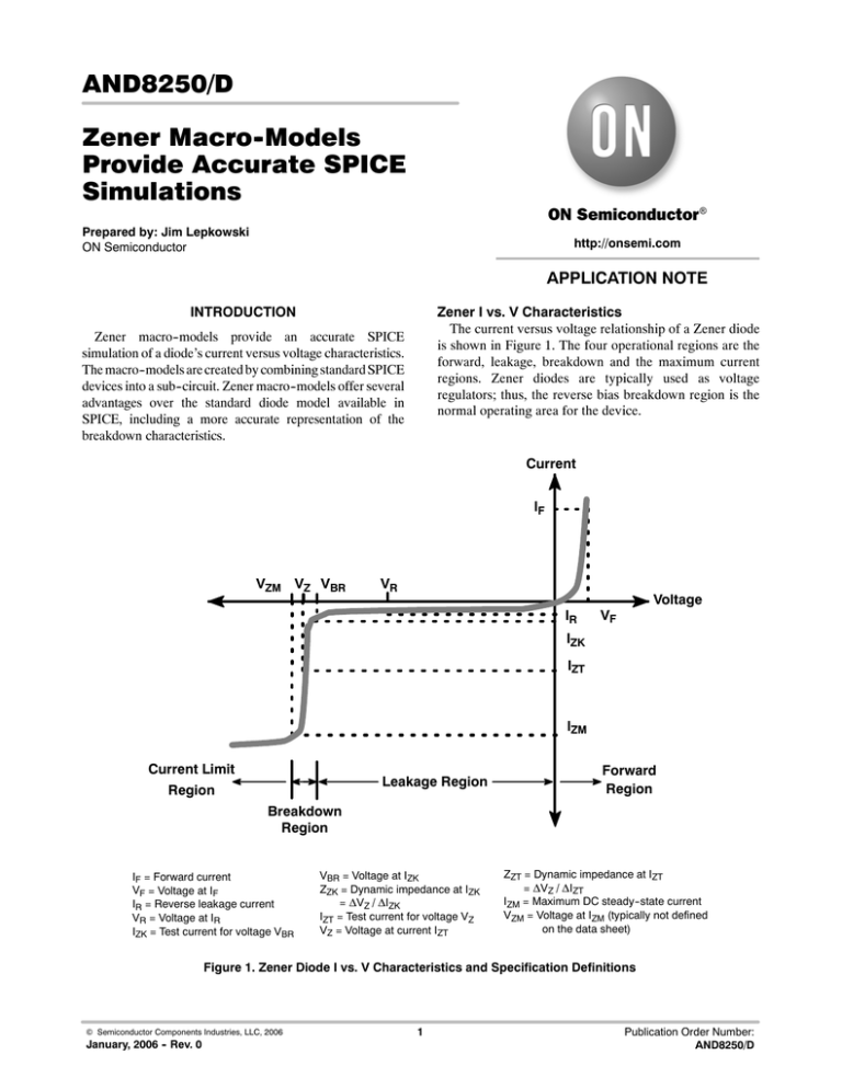
The current versus voltage relationship of a Zener diode
is shown in Figure 1. The four operational regions are the
forward, leakage, breakdown and the maximum current
regions. Zener diodes are typically used as voltage
regulators; thus, the reverse bias breakdown region is the
normal operating area for the device.
INTRODUCTION
Zener macro--models provide an accurate SPICE
simulation of a diode’s current versus voltage characteristics.
The macro--models are created by combining standard SPICE
devices into a sub--circuit. Zener macro--models offer several
advantages over the standard diode model available in
SPICE, including a more accurate representation of the
breakdown characteristics.
Current
IF
VZM VZ VBR
VR
IR
Voltage
VF
IZK
IZT
IZM
Current Limit
Leakage Region
Region
Forward
Region
Breakdown
Region
IF = Forward current
VF = Voltage at IF
IR = Reverse leakage current
VR = Voltage at IR
IZK = Test current for voltage VBR
VBR = Voltage at IZK
ZZK = Dynamic impedance at IZK
= ΔVZ / ΔIZK
IZT = Test current for voltage VZ
VZ = Voltage at current IZT
ZZT = Dynamic impedance at IZT
= ΔVZ / ΔIZT
IZM = Maximum DC steady--state current
VZM = Voltage at IZM (typically not defined
on the data sheet)
Figure 1. Zener Diode I vs. V Characteristics and Specification Definitions
© Semiconductor Components Industries, LLC, 2006
January, 2006 -- Rev. 0
1
Publication Order Number:
AND8250/D
AND8250/D
Zener Diode SPICE Model Options
The three basic methods used to create Zener diode SPICE
models are listed below.
1. Curve Fit Models
2. SPICE Diode Statement
3. Macro--Model Subcircuit
SPICE Diode Statement
Curve Fit Models
* anode cathode model name
D1 2
1
MD1
The majority of the Zener SPICE models available in the
industry are created using the SPICE ‘D’ diode statement.
Table 1 provides the variables available with the PSPICE
‘D’ diode model. An example of a ‘D’ statement is shown
below.
Curve fit SPICE models are an attractive modeling option
in versions of SPICE that have analog behavior modeling
statements. The mathematical functions and “If--Then--Else”
commands can be used to perform conditional branching to
accurately match the Zener’s impedance in the four operating
regions. Curve fit models are not as popular as the Diode ‘D’
statement or macro--model options because the analog
behavioral statements are not available in some versions of
SPICE. In contrast, the SPICE statements used in the diode
and macro--model are compatible with almost all versions of
SPICE.
Curve fit models are created using a polynomial
expression in the SPICE voltage controlled current source
‘G’ command. The polynomials can be generated using the
curve fit feature of a mathematical program such as
MathCad or Excel to form a transfer function of the Zener’s
impedance. A negative feature of the curve fit approach is
that this option creates a mathematical model, while in
contrast the macro--model approach produces an equivalent
circuit to represent the Zener.
.MODEL MD1 D IS=6.57933e--10 N=1.84949 XTI=1
+RS=1.022CJO=1.5e--10 TT=1e--08
There are several restrictions that limit the accuracy of
using the diode ‘D’ statement to model a Zener. First, the
diode statement does not have a provision for defining a
separate series resistance for the forward and reverse bias
breakdown regions. The resistances in the two regions are
not equal; thus, it is not possible to accurately model the
slope of the voltage versus current characteristic in both
regions. Next, the ‘D’ statement does not have a variable to
model the variance of the Zener voltage with temperature
(T). The polarity and magnitude of ΔVZ/ΔT is a function
of the breakdown voltage. If VZ is < 5.6 V, ΔVZ/ΔT ≈
--2.0 mV/_C. If VZ is > than 5.6 V, the ΔVZ/ΔT temperature
coefficient is positive and increases as a function of the
magnitude of VZ. Also, the diode statement does not have a
variable to limit the current to a maximum value that
matches the Zener’s power dissipation capability.
Table 1. Default Values of the PSPICE Diode Statement ‘D’ Variables
Variable
Parameter
SPICE Default
Value
ON
Macro--Model
Default Value
Units
1 E--14
1 E--14
A
IS
Saturation Current
RS
Resistance
0
10
Ω
BV
Reverse Breakdown Voltage
∞
5
V
IBV
Current at Reverse Breakdown Voltage
1 E--3
1 E--3
A
Emission Coefficient (η)
1
1
--
Saturation Current Temp. Coefficient
3
0
--
Transit Time
0
10
nS
Zero Bias Junction Capacitance
0
50
pF
VJ
Junction Potential
1
1
V
M
Grading Coefficient
0.5
0.5
--
EG
Activation Energy
1.11
1.11
eV
KF
Flicker Noise Coefficient
0
0
--
AF
Flicker Noise Exponent
1
1
--
FC
Depletion Capacitance Forward Bias Coefficient
0.5
0.5
--
Nominal Temperature
27
27
_C
N
XT1
TT
CJO
TNOM
1. The values of the ON macro--model components are generated by the MODPEX software from the data sheet specifications.
2. The PSPICE diode command does not have a maximum current limit (IMAX) variable. The macro--model’s default value for IZM is 200 mA.
3. The PSPICE diode command does not have a variable to define the temperature coefficient of the breakdown voltage. The macro--model’s
default value for ΔVZ/ΔT is 0 mV/_C.
http://onsemi.com
2
AND8250/D
Macro--Model Subcircuit
A Zener diode macro--model can be created using
standard SPICE components. Figure 2 shows a schematic
representation of the macro--model that is used to create the
majority of the ON Zener SPICE models. The netlist for the
MMBZ5232’s macro--model is provided in Appendix I as
an example. A summary of the operation of the model is
given in Table 2. Further details on the macro--model are
provided in references [5] and [6]. Alternative Zener diode
macro--models are given in references [1]--[4].
Anode
I D = IF + IL + IR
2
Anode
+
2
ID
VD
--
1
Cathode
IR
RZ
IF
IL
D1
RL
3
D3
IZG
RZG
4
D2
-+
EV1
1
5
EV1 = VBR = IBV x RBV
IBV
6
RBV
0
+
EV1
--
Cathode
Figure 2. Zener Diode SPICE Macro--Model
Forward Bias Region
Diode D1 is the key component when the voltage VD
across the Zener is greater than zero. D1’s forward bias
characteristics are controlled by the saturation (IS),
emission coefficient (N) and series resistance (RS)
variables. The forward bias current equations are listed
below.
ID = IF + IL + IR
V
= IF_D1 + D + IS_D2
RL
IL & IR ≪ IF_D1
∴ID ≅ IF_D1 ≅ IS_D1 e ^
VD1
VD1
− 1 ≅ IS_D1 e ^
ηVT
ηVT
VT = kT
q ≅ 26 mV @ 25˚C
Leakage Region
The leakage or reverse bias before breakdown region is
defined when voltage VD is between 0 V and the
breakdown voltage (VBR). Currents IF and IR are small in
comparison to IL because diodes D1 and D2 are reverse
biased. The leakage current can be approximated by the
ratio of VD to RL.
ID = IF + IL + IR
V
= IS_D1 + D − IS_D2
RL
VD
∴ID ≅
RL
IS_D1 & IS_D2 ≪ IL
Breakdown Region
(VBR), represented by EV1, is equal to the product of current
source IBV and resistor RBV. The Zener voltage VZ,
specified at current IZT, is equal to the sum of the voltages of
EV1, RZ, D2 and D3 as shown below.
The reverse bias breakdown region is modeled by the
devices contained in the current path of IR. Current flows
through this path when voltage VD exceeds the voltage of
EV1 plus the forward voltage of D2. The breakdown voltage
VD
I
∴VD ≅ ηVT In D
ηVT
IS
VZ = VBR + VD2 + VRZ − VD3
ID ≅ IS e ^
I
I
VZ @ IZT = EV1 + η2VT ln D2 + (IZTRZ) − η3VT ln D3
IS3
IS2
I --I
IZT
= (IBRRBV) + η2VT ln
+ (IZTRZ) − η3VT ln ZG ZT
IS2
IS3
http://onsemi.com
3
AND8250/D
Current Limit Region
An equation that determines the ratio of the emission
coefficients η2 and η3 is created by assuming that the reverse
saturation currents for diodes D2 and D3 are equal.
I --I
η3 = η2 ln ZG ZT
IZT
Diode D3, current source IZG and resistor RZG are used to
form a current limiting circuit. The current limiting mode
occurs when ID2 increases to the value of IZG, which reverse
biases D3 and limits the current. The maximum current
(IZM) has a weak dependency on the magnitude of the bias
voltage and RZG is used to provide a slope to the current
versus voltage curve. D3’s current can be expressed by the
equations listed below.
The Zener impedance, or the slope of the current versus
voltage curve, is equal to the derivative of the diode’s
voltage equation with respect to current. The impedance
equation shown below is valid for low frequencies, where
the junction capacitance can be neglected.
ZD =
ID3 = IZG − ID2 − IRZG
IRZG ≪ IZG & ID2
ηVT
δVD
=
ID
δID
∴ID3 ≅ IZG − ID2
The impedance of the Zener, defined as ZZT and ZZK, is
defined at test currents IZT and IZK, respectively. The two
impedance and η3 equations are used to calculate RZ, η2 and
η3. The Zener impedance in the breakdown region is
approximated by neglecting the parallel connected resistor
RL and the reverse biased diode D1 for simplicity.
Macro--Model Limitations
Macro--models provide an accurate SPICE representation
of a Zener’s current and voltage characteristics for most
applications. The macro--models solve several of the
limitations associated with the SPICE diode ‘D’ statement
and the curve fit models. The accuracy of the macro--models
is directly proportional to the thoroughness of the Zener’s
data sheet. Macro--models are a powerful analytical design
tool; however, they should not be used as a replacement for
hardware development tests. A summary of the limitations
of the macro--models is shown in Table 3.
ZZ ≅ RZ + ZD2 + ZD3
ZZT ≅ RZ +
η2VT
η3VT
+
(IZG --IZT)
IZT
ZZK ≅ RZ +
η2VT
η3VT
+
(IZG --IZK)
IZK
Table 2. Key Design Equations and Features of the Zener Diode Macro--Model
Region
Forward
Bias
Voltage
Boundaries
VD > 0
Macro--Model
Components
Key Design Equations
ID ≅ IF_D1 ≅ IS_D1 e ^
D1
VD1
ηVT
Comments
•
ID is defined by the Ebers--Moll
equation
•
D1’s RS variable models the ΔI/ΔV
slope
Leakage
Region
VBR < VD ≤ 0
V
ID ≅ IL ≅ D
RL
RL
•
RL’s temperature coefficients model
ΔIL/ΔT
Breakdown
VZM < VD ≤ VBR
VZ ≅ VZT + ZZTID
VZT = VZ @ IZT
ZZT ≅ RZ + RSD2 + RSD3
EV1, D2, RZ
IBV, RBV
•
The recommended bias current for a
voltage regulator application is IZM < ID
≤ IZT
•
•
Current
Limit
VD ≤ VZM
D3, IZG, RZG
IZM ≅ IZG
http://onsemi.com
4
•
•
RBV’s temperature coefficients model
ΔVZ/ΔT
RZ models the ΔI/ΔV slope
IZM is a function of the IC package
RZG models the ΔI/ΔV slope
AND8250/D
Table 3. Simulation Limits of Zener Macro--Models
Region
Key Design Parameter
Forward
Forward Voltage (VF)
Leakage
Breakdown
Current Limit
Leakage Current (IL)
Zener Voltage (VZ)
Maximum Current (IMAX)
Model Limitation
•
VF is typically specified as a maximum value at a single current point in the data
sheet
•
The simulation accuracy is enhanced if two typical current points are used by the
modeling algorithm
•
•
IL is modeled as a linear function of the bias voltage
•
•
VZ tolerance (typ. 5%) is not modeled
•
•
•
Voltage surge suppression capability beyond IMAX is not modeled
IL actually varies as an exponential function of the bias voltage
Monte--Carlo simulations can provide tolerance and worst case analysis
Thermal self--heating produced when ID is large is not modeled
Device overcurrent failures are not modeled. At the device’s destruction point, VZ
‘collapses’ or decreases to a low value, which increases the current through the
device to a level that damages the device
References
1. Antognetti, P. and Massobrio, G., “Semiconductor
Device Modeling with Spice”, McGraw--Hill, New
York, 1990.
2. Deveney, M., “A Temperature Dependent SPICE
Macro--Model for Zener and Avalanche Diodes”,
IEEE Circuits and Systems Midwest Symposium,
May, 1991.
3. Pawlikiewicz, A. and Zack, G., “A New
Macro--Model for Zeners”, IEEE Circuits and
Devices Magazine, Volume 9, Issue 2, March,
1993.
4. Sandler, S., “SPICE Subcircuit Accurately Models
Zener Characteristics”, Personal Engineering,
November, 1998.
5. Wong, S. and Hu, C., “SPICE Macro--Model for
the Simulation of Zener Diode I--V
Characteristics”, IEEE Circuits and Devices
Magazine, Volume 7, Issue 4, July, 1991.
6. Wong, S., Hu, C. and Chan, S., “SPICE
Macro--Model for the Simulation of Zener Diode
Current--Voltage Characteristics”, International
Journal of Electronics, Volume 71, No. 24, August,
1991.
http://onsemi.com
5
AND8250/D
Appendix I: MMBZ5232B Zener Diode Macro--Model SPICE Netlist
**********************************************************************************
*
MMBZ5232B Macro--Model SPICE Model
*
Model Generated by MODPEX
*
Copyright(c) Symmetry Design Systems
*
All Rights Reserved
*
MODEL FORMAT: PSPICE
****************************************************************************
*
node:
anode cathode
.SUBCKT mmbz5232blt1 2
1
**********************************************************************************
*
Forward Region
*
D1’s CJO term models the Zener’s capacitance
D1 2 1 MD1
.MODEL MD1 D IS=7.58703e--07 N=3.10159 XTI=1 RS=0.856
+ CJO=1.5e--10 TT=1e--08
****************************************************************************
*
Leakage Region
*
RL models leakage current (IL)
*
MDR temp. coef. model ∆IL / ∆T
RL 1 2 MDR 1.5e+09
.MODEL MDR RES TC1=0 TC2=0
****************************************************************************
*
Reverse Breakdown Region
*
RZ models the ∆I / ∆V slope
RZ 2 3 0.862776
D2 5 4 MD2
.MODEL MD2 D IS=2.5e--12 N=0.475376 XTI=0 EG=0.1
EV1 1 5 6 0 1
*
Breakdown Voltage (VBR) = IBV x RBV
*
MDRBV temp. coef. model ∆VBR / ∆T
IBV 0 6 0.001
RBV 6 0 MDRBV 5431.8
.MODEL MDRBV RES TC1=0.000368055
****************************************************************************
*
Current Limit Region
*
Maximum current (IZM) is set to magnitude of IZG
*
RZG models the ∆I / ∆V slope
IZG 4 3 0.24
RZG 4 3 75
D3 3 4 MD3
.MODEL MD3 D IS=2.5e--12 N=0.198247 XTI=0 EG=0.1
*
.ENDS mmbz5232blt1
****************************************************************************
http://onsemi.com
6
AND8250/D
ON Semiconductor and
are registered trademarks of Semiconductor Components Industries, LLC (SCILLC). SCILLC reserves the right to make changes without further notice
to any products herein. SCILLC makes no warranty, representation or guarantee regarding the suitability of its products for any particular purpose, nor does SCILLC assume any liability
arising out of the application or use of any product or circuit, and specifically disclaims any and all liability, including without limitation special, consequential or incidental damages.
“Typical” parameters which may be provided in SCILLC data sheets and/or specifications can and do vary in different applications and actual performance may vary over time. All
operating parameters, including “Typicals” must be validated for each customer application by customer’s technical experts. SCILLC does not convey any license under its patent rights
nor the rights of others. SCILLC products are not designed, intended, or authorized for use as components in systems intended for surgical implant into the body, or other applications
intended to support or sustain life, or for any other application in which the failure of the SCILLC product could create a situation where personal injury or death may occur. Should
Buyer purchase or use SCILLC products for any such unintended or unauthorized application, Buyer shall indemnify and hold SCILLC and its officers, employees, subsidiaries, affiliates,
and distributors harmless against all claims, costs, damages, and expenses, and reasonable attorney fees arising out of, directly or indirectly, any claim of personal injury or death
associated with such unintended or unauthorized use, even if such claim alleges that SCILLC was negligent regarding the design or manufacture of the part. SCILLC is an Equal
Opportunity/Affirmative Action Employer. This literature is subject to all applicable copyright laws and is not for resale in any manner.
PUBLICATION ORDERING INFORMATION
LITERATURE FULFILLMENT:
N. American Technical Support: 800--282--9855 Toll Free
Literature Distribution Center for ON Semiconductor
USA/Canada
P.O. Box 61312, Phoenix, Arizona 85082--1312 USA
Phone: 480--829--7710 or 800--344--3860 Toll Free USA/Canada Japan: ON Semiconductor, Japan Customer Focus Center
2--9--1 Kamimeguro, Meguro--ku, Tokyo, Japan 153--0051
Fax: 480--829--7709 or 800--344--3867 Toll Free USA/Canada
Phone: 81--3--5773--3850
Email: orderlit@onsemi.com
http://onsemi.com
7
ON Semiconductor Website: http://onsemi.com
Order Literature: http://www.onsemi.com/litorder
For additional information, please contact your
local Sales Representative.
AND8250/D
