DS2187 Receive Line Interface
advertisement

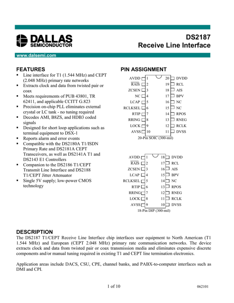
DS2187 Receive Line Interface www.dalsemi.com FEATURES PIN ASSIGNMENT Line interface for T1 (1.544 MHz) and CEPT (2.048 MHz) primary rate networks Extracts clock and data from twisted pair or coax Meets requirements of PUB 43801, TR 62411, and applicable CCITT G.823 Precision on-chip PLL eliminates external crystal or LC tank - no tuning required Decodes AMI, B8ZS, and HDB3 coded signals Designed for short loop applications such as terminal equipment to DSX-1 Reports alarm and error events Compatible with the DS2180A T1/ISDN Primary Rate and DS2181A CEPT Transceivers, as well as DS2141A T1 and DS2143 E1 Controllers Companion to the DS2186 T1/CEPT Transmit Line Interface and DS2188 T1/CEPT Jitter Attenuator Single 5V supply; low-power CMOS technology AVDD 1 20 DVDD RAIS 2 19 RCL ZCSEN 3 18 AIS NC 4 17 BPV LCAP 5 16 NC RCLKSEL 6 15 NC RTIP 7 14 RPOS RRING 8 13 RNEG LOCK 9 12 RCLK AVSS 10 11 DVSS 20-Pin SOIC (300-mil) AVDD 1 18 DVDD RAIS 2 17 RCL ZCSEN 3 16 AIS LCAP 4 15 BPV RCLKSEL 5 14 NC RTIP 6 13 RPOS RRING 7 12 RNEG LOCK 8 11 RCLK AVSS 9 10 DVSS 18-Pin DIP (300-mil) DESCRIPTION The DS2187 T1/CEPT Receive Line Interface chip interfaces user equipment to North American (T1 1.544 MHz) and European (CEPT 2.048 MHz) primary rate communication networks. The device extracts clock and data from twisted pair or coax transmission media and eliminates expensive discrete components and/or manual tuning required in existing T1 and CEPT line termination electronics. Application areas include DACS, CSU, CPE, channel banks, and PABX-to-computer interfaces such as DMI and CPI. 1 of 10 062101 DS2187 DS2187 BLOCK DIAGRAM Figure 1 LINE INPUT Input signals are coupled to the DS2187 via a 1:2 center-tapped transformer as shown in Figure 2. For T1 applications, R1 and R2 must be 200 ohms in order to properly terminate the line at 100 ohms. R1 and R2 are set at 150 or 240 ohms for CEPT applications. Special internal circuitry of the RTIP and RRING inputs permits negative signal excursions below VSS, which will occur in the circuit in Figure 2. PEAK DETECTOR AND SLICERS Signal pulses present at RTIP and RRING are sampled by an internal peak detect circuit. The clock and data slicer threshold are set for 50% of the sampled peak voltage. Peak input levels at RRIP and RRING must exceed 0.6 volts to establish minimum slicer thresholds. Signals below this level will cause RCL to transition high after 192 bit times. CLOCK EXTRACTION The DS2187 utilizes both frequency locked (FLL) and digital phase locked (DPLL) loops to recover data and clock from the incoming AMI signal. T1 applications utilize a 18.528 MHz clock divided by either 11, 12, or 13 to match the phase of the incoming jittered line signal. This technique affords exceptional jitter tracking which enables the DS2187 to meet the latest AT&T TR 62411 and ECSA jitter specifications. A 24.576 MHz clock divided by 11, 12, or 13 provides jitter tracking in the CEPT mode. The DPLL output is buffered and presented at RCLK. An on-chip, laser-trimmed, voltage-controlled oscillator (VCO) provides the precision 18.528 MHz and 24.576 MHz frequency sources utilized in the FLL. The FLL is a high-Q circuit which tracks the average frequency of the incoming signal, minimizing the effect of the DPLL on output jitter. During the acquisition time or if RCL goes high, the LOCK pin will go low to indicate a loss of synchronization to the line signal. Once this pin goes high, the FLL has achieved frequency lock and valid data is present at the RPOS and RNEG outputs. 2 of 10 DS2187 PIN DESCRIPTION Table 1 PIN SYMBOL TYPE 1 2 AVDD RAIS I 3 ZCSEN I 4 LCAP - 5 RCLKSEL I 6 7 8 RTIP RRING LOCK I 9 10 11 12 13 14 15 AVSS DVSS RCLK RNEG RPOS NC BPV O 16 AIS O 17 RCL O 18 DVDD - O O O DESCRIPTION Analog Positive Supply. 5.0 volts. Reset Alarm Indication Signal. Every other low pulse at this input establishes the AIS alarm detection period. 0 Code Suppression Enable. When high, incoming B8ZS (RCLKSEL=0) or HDB3 (RCLKSEL=1) code words are replaced with all 0s at RPOS and RNEG; when low, no code replacement occurs. Loop Cap. Part of internal loop filter; attach a 10 microfarad capacitor from this pin to VSS. Receive Clock Select. Tie to VSS for 1.544 MHz (T1) applications, to VDD for 2.048 MHz (CEPT) applications. Receive Tip and Ring. Connect to line transformer as shown in Figure 2. Frequency Lock. High state indicates that internal circuitry is phase- and frequency-locked to the incoming signal at RRING and RTIP. Analog Signal Ground. 0.0 volts. Digital Signal Ground. 0.0 volts. Receive Clock. Extracted line rate clock. Receive Data. Extracted receive data; updated on rising edge of RCLK. No Connect. Do not connect to this pin. Bipolar Violation. Transitions high for the full bit period when a bit in violation appears at RPOS or RNEG; B8ZS code words are not accused when ZCSEN=1. BPV not valid for RCLKSEL=1 and ZCSEN=1. Alarm Indication Signal. High when the received data stream has contained less than three 0s during the last two periods of the RAIS signal. Receive Carrier Loss. High if 192 0s appear at RPOS and RNEG; reset on next occurrence of a one. Digital Positive Supply. 5.0 volts 3 of 10 DS2187 SYSTEM LEVEL INTERCONNECT Figure 2 OUTPUT TIMING Figure 3 4 of 10 DS2187 0 CODE SUPPRESSION The device will decode incoming B8ZS (RCLKSEL=0) or HDB3 (RCLKSEL=1) code words and replace them with an all-0 code when ZCSEN=1. When ZCSEN=0, code words will pass through the device without being altered. This feature can be disabled when the DS2187 is used with transceiver devices such as the DS2180A DS2181A, DS2141A, or DS2143. ALARM DETECTION The extracted data is monitored for network alarm and error conditions. RCL is set when 192 consecutive 0s occur; it is cleared on the next one occurrence. AIS is set when less than three 0s have appeared at RPOS and RNEG during the last two periods of the RAIS signal; once set, AIS will remain high for the next two periods of RAIS . AIS will return low when more than two 0s appear. BPV reports bipolar violations as they occur at RPOS and RNEG; B8ZS code words will not be flagged by BPV when ZCSEN=1. BYPASSING AND LAYOUT CONSIDERATIONS The DS2187 contains both precision analog and high-speed digital circuitry on the same chip. The power supplies of these circuits (AVDD, AVSS, DVDD and DVSS) should be connected to system analog and digital supplies. If separate system supplies do not exist, the appropriate supply pins can be tied together. Tying the analog and digital supplies together on the DS2187 will not degrade its performance, provided the power supply is sufficiently decoupled. To assure optimum performance, the length of LCAP, RTIP and RRING printed circuit board traces should be minimized and isolated from neighboring interconnect. 5 of 10 DS2187 ABSOLUTE MAXIMUM RATINGS* Voltage on Any Pin Relative to Ground Operating Temperature Storage Temperature Soldering Temperature -0.1V to +7.0V 0° to 70°C -55°C to +125°C 260°C for 10 seconds * This is a stress rating only and functional operation of the device at these or any other conditions above those indicated in the operation sections of this specification is not implied. Exposure to absolute maximum rating conditions for extended periods of time may affect reliability. ** Inputs other than RTIP and RRING RECOMMENDED DC OPERATING CONDITIONS PARAMETER SYMBOL MIN Input Logic 1 VIH Input Logic 0 TYP (0°C to 70°C) MAX UNITS NOTES 2.0 VCC+.3 V 1 VIL -0.3 +0.8 V 1 Supply VDD 4.75 5.25 V Input Voltage Swing RTIP,RRING VIN -7.0 12.0 V DC ELECTRICAL CHARACTERISTICS PARAMETER SYMBOL MIN (0°C to 70°C) TYP MAX UNITS NOTES 18 25 mA 2 +10 µA 1, 3 Supply Current IDD Input Leakage IL -1.0 Output Current @ 2.4V IOH -1.0 mA 4 Output Current @ 0.4V IOL +4.0 mA 4 NOTES: 1. All inputs except RTIP and RRING. 2. Outputs open. 3. 0.0V < VIN <VDD. 4. All outputs. 6 of 10 DS2187 ANALOG ELECTRICAL CHARACTERISTICS PARAMETER Clock Acquisition SYMBOL MIN (0°C to 70°C; VDD = 5.0V ± 5%) TYP MAX UNITS NOTES ms 1 Vpk 2 tLOCK 50 VTHRES .4 FLL Loop Bandwidth fBW 50 Hz 3 Capture Range fCAP ±6 % 4 Input Jitter Tolerance JIN UI 5 RTIP, RRING Minimum Sensitivity .6 200 NOTES: 1. Time from reappearance of a valid signal at RPOS and RNEG to a LOCK=1. 2. Minimum peak voltage necessary for proper processing of signal. 3. Loop bandwidth when in lock (LOCK=1). 4. When out of lock (LOCK=0), measured as a percent of incoming clock frequency. 5. Maximum input jitter in unit intervals at 10 Hz. CAPACITANCE PARAMETER Input Capacitance Output Capacitance (TA = 25°C) SYMBOL MIN MAX UNITS CIN 5 pF COUT 7 pF AC ELECTRICAL CHARACTERISTICS PARAMETER RCLK Period RCLK Period RCLK Pulse Width RCLK Pulse Width RCLK Rise and Fall Times Propagation delay RCLK TO RPOS, RNEG Propagation delay RCLK to BPV, RCL, AIS RAIS Setup TYP NOTES (0°C to 70°C; VDD = 5.0V ± 5%) SYMBOL MIN TYP MAX UNITS NOTES tRCLK tRCLK tRWH, tRWL tRWH, tRWL tR, tF tPRD 594 445 648 488 324 702 530 ns ns ns 1,3 2,3 1 ns 2 244 tPRA tSU, tHD 50 7 of 10 20 75 ns ns 75 ns ns DS2187 NOTES: 1. T1 applications (RCLKSEL=0). 2. CEPT applications (RCLKSEL=1). 3. Minimum and maximum limits shown reflect changes in DPLL divide ratio as required to track jitter. AC TIMING DIAGRAM Figure 4 8 of 10 DS2187 DS2187 RECEIVE LINE INTERFACE 18-PIN DIP PKG DIM A IN MM B IN MM C IN MM D IN MM E IN MM F IN MM G IN MM H IN MM J IN MM K IN MM 18-PIN MIN MAX 0.890 0.920 0.240 6.10 0.120 3.05 0.300 7.62 0.015 0.38 0.120 3.04 0.090 2.23 0.320 8.13 0.008 0.20 0.015 0.38 0.260 6.60 0.140 3.56 0.325 8.26 0.040 1.02 0.140 3.56 0.110 2.79 0.370 9.40 0.012 0.30 0.021 0.53 9 of 10 DS2187 DS2187S RECEIVE LINE INTERFACE 20-PIN SOIC PKG DIM A IN MM B IN MM C IN MM E IN MM F IN MM G IN MM H IN MM J IN MM K IN MM L IN MM phi 18-PIN MIN MAX 0.500 0.511 12.70 12.99 0.290 0.300 7.37 7.65 0.089 0.095 2.26 2.41 0.004 0.012 0.102 0.30 0.094 0.105 2.38 2.68 0.050 BSC 1.27 BSC 0.398 0.416 10.11 10.57 0.009 0.013 0.229 0.33 0.013 0.019 0.33 0.48 0.016 0.040 0.406 1.20 0° 8° 10 of 10


