UV6™ POSITIVE DUV
PHOTORESIST
For DUV Applications
σ)
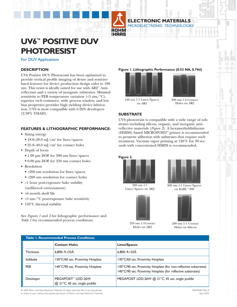
Figure 1. Lithographic Performance (0.53 NA, 0.74σ
DESCRIPTION
UV6 Positive DUV Photoresist has been optimized to
provide vertical profile imaging of dense and semi-isolated features for device production design rules to 180
nm. This resist is ideally suited for use with AR2™ Antireflectant and a variety of inorganic substrates. Minimal
sensitivity to PEB temperature variation (<5 nm/°C),
superior etch resistance, wide process window, and low
bias properties provides high yielding device fabrication. UV6 is most compatible with 0.26N developers
(2.38% TMAH).
FEATURES & LITHOGRAPHIC PERFORMANCE:
• Sizing energy
• 18.0–28.0 mJ/cm2 for lines/spaces
• 25.0–40.0 mJ/cm2 for contact holes
• Depth of focus
• 1.00 µm DOF for 200 nm lines/spaces
• 0.80 µm DOF for 250 nm contact holes
• Resolution
• <200 nm resolution for lines/spaces
• <200 nm resolution for contact holes
• >1 hour post-exposure bake stability
(unfiltered environment)
• >6 month shelf life
• <5 nm/°C post-exposure bake sensitivity
• 150°C thermal stability
See Figures 1 and 2 for lithographic performance and
Table 1 for recommended process conditions.
180 nm 1:1 Lines/Spaces
on AR2
200 nm 1:2 Contact
Holes on AR2
SUBSTRATE
UV6 photoresist is compatible with a wide range of substrates including silicon, organic, and inorganic antireflective materials (Figure 2). A hexamethyldisilazane
(HMDS) based MICROPOSIT® primer is recommended
to promote adhesion with substrates that require such
treatment. Vacuum vapor priming at 120°C for 30 seconds with concentrated HMDS is recommended.
Figure 2.
200 nm 1:1
Lines/Spaces on AR2
250 nm 1:1Contact
Holes on AR2
200 nm 1:1 Lines/Spaces
on BARL™ 900
200 nm 1:1 Contact
Holes on Silicon
Table 1. Recommended Process Conditions
Contact Holes
Lines/Spaces
Thickness
6,800–9,125Å
6,800–9,125Å
Softbake
130°C/60 sec. Proximity Hotplate
130°C/60 sec. Proximity Hotplate
PEB
140°C/90 sec. Proximity Hotplate
130°C/90 sec. Proximity Hotplate (for non-reflective substrates)
140°C/90 sec. Proximity Hotplate (for reflective substrates)
Developer
MEGAPOSIT™ LDD-26W
@ 21°C, 45 sec. single puddle
MEGAPOSIT LDD-26W @ 21°C, 45 sec. single puddle
© 2004 Rohm and Haas Electronic Materials. All rights reserved. Not to be reproduced,
in whole or part, without the express permission of Rohm and Haas Electronic Materials.
ME04N087, Rev. 0
April 2004
2
UV6 POSITIVE DUV PHOTORESIST
COAT
Figure 4. Dispersion Curve
Figure 3 shows the relation between spin speed and
resist thickness for 6-inch substrates. Nominal film
thickness may vary slightly due to process, equipment
and ambient conditions.
Figure 3. Spin Speed Curves
Table 3. Cauchy Coefficients
n1
1.5612
n2
-1.0297e5
n3
1.5492e13
Figure 5. Interference Curves - Bulk E0
SOFTBAKE
The recommended softbake process for lines/ spaces
and contact holes is listed in Table 2 for silicon and antireflective substrates.
Table 2. Softbake Process Conditions
Contact Holes
Lines/Spaces and
Isolated Lines
Temperature 130°C
130°C
Time
60 sec. Proximity
Hotplate
60 sec. Proximity
Hotplate
Figure 6. Interference Curves—
250 nm 1:1 Lines/Spaces CD
FILM THICKNESS MEASUREMENT
Figure 4 shows the refractive index of UV6 as a function
of wavelength. Cauchy coefficients are listed in Table 3.
Resist thicknesses of 6,800–9,125Å were used to characterize UV6. Figures 5 and 6 display the E0 and CD interference curves for silicon, BARL 900 and AR2.
3
UV6 POSITIVE DUV PHOTORESIST
EXPOSE
Table 5. Post-exposure Bake Process Conditions
Figure 7 displays the absorbance curve for the unexposed resist film. Table 4 lists the parameters needed for
resist modeling.
Lines/Spaces
Contact
Holes
Temperature 140°C (Reflective Substrates)
140°C
130°C (Anti-Reflectant Substrates)
Figure 7.Absorbance Curve
Absorbance
Time
90 sec. Proximity Hotplate
Figure 8. PEB Sensitivity
Wavelength (nm)
Table 4. Prolith Parameters
Dill A Value
0.13053
Dill B Value
0.6016
Dill C Value
0.0257 cm2/mJ
Rmin
0.49 Å/sec.
Rmax
3,841 Å/sec.
Acid Generation Coefficient
0.051 cm2/mJ
n
6.78
RI @ 633 nm
1.57
RI @ 248 nm
1.70
POST-EXPOSURE DELAY STABILITY
As shown in Figure 9, the delay stability for UV6 is
greater than 1 hour in a non-filtered environment.
Figure 9. Delay Stability on BARL 900
No Delay
1 Hour Delay
*Chemically-amplified resists require additional modeling
parameters currently being determined. Please see your TSR
for an updated copy of modeling parameters.
POST-EXPOSURE BAKE
A 10-degree temperature differential (softbake lower
then PEB) is used to reduce standing waves on reflective substrates. On non-reflective substrates, no temperature difference is required. The recommended processing conditions for reflective and non-reflective substrates are listed in Table 5. Figure 8 shows the PEB sensitivity of UV6.
250 nm 1:1 Lines/Spaces in a non-filtered environment.
DEVELOP
UV6 is optimized for 0.26N developers (Figure 10, next
page). A 45 second single puddle with no pre-wet is recommended for most applications including lines/spaces
and contact holes. Figure 11 (next page) shows the dissolution rate as a function of exposure dose.
4
UV6 POSITIVE DUV PHOTORESIST
Figure 10. Developer Compatibility
200 nm 1:1 Lines/Spaces
LDD-26W
Figure 12.Thermal Flow Characteristics
250 nm 1:1 Lines/Spaces
MF-926HS
No Bake
MF-86MX
NMD-W
140°C/3 min.
Figure 11. Dissolution Curve on Silicon
145°C/3 min.
HARDBAKE
Figure 12 displays the thermal flow characteristics of
UV6 photoresist.
150°C/3 min.
155°C/3 min.
10 µm Pad
5
UV6 POSITIVE DUV PHOTORESIST
PHOTORESIST REMOVAL
HANDLING PRECAUTIONS
UV6 can be removed with MICROPOSIT REMOVER
1165®. A two-bath process is recommended with each
bath at a temperature of 80°C. The first bath removes
the bulk of the photoresist and the second removes
residual traces of photoresist. Please consult specific
remover datasheets for additional process information.
UV6 is a combustible liquid and vapor; keep away from
heat sparks and open flame. Irritation to eyes, nose and
respiratory track can occur. Use with adequate ventilation and avoid breathing vapors and mists. Wash thoroughly after handling and always wear chemical goggles, gloves, and suitable protective clothing. In case of
eye or skin contact, flush affected areas with plenty of
water for at least 15 minutes.
ETCH RESISTANCE
Contact a physician at once. Consult Product Material
Safety Data Sheet before using.
Figure 13 shows the etch performance of UV6 with a
chlorine-based metal etch process. Blanket etch studies
performed in an Applied Materials, Inc. Model 5000
etcher.
Figure 13. Etch Resistance
WASTE TREATMENT
UV6 contains ethyl lactate and may be included with
other wastes containing similar organic solvents to be
discarded for destruction or reclaim in accordance with
local, state, and federal regulations.
It is your responsibility to ensure the disposal of UV6
and residues therefrom is made in compliance with all
applicable environmental regulations.
STORAGE
Store UV6 only in upright, sealed, original containers in
a dry area at 30–50°F (-1–10°C) away from heat and
sunlight. Keep away from alkaline materials, acids and
oxidizers. Keep container closed when not in use.
6
UV6 POSITIVE DUV PHOTORESIST
Circuit Board Technologies
CMP Technologies
Microelectronic Technologies
Packaging and Finishing Technologies
For locations and information please visit; http://electronicmaterials.rohmhaas.com
APEX-E, AR2, BARL, UV6, MEGAPOSIT, MICROPOSIT, Rohm and Haas, and Rohm and Haas Electronic Materials are trademarks of Rohm and Haas Company, Philadelphia,
PA, USA, or its affiliates.
UNITED STATES
JAPAN
ASIA
EUROPE
Marlborough, MA
Tokyo
Hong Kong
Paris, France
Tel: 800.832.6200
Tel: +81.3.5213.2910
Tel: +852.2680.6888
Tel: +33.1.40.02.54.00
Fax: 508.485.9113
Fax: +81.3.5213.2911
Fax: +852.2680.6333
Fax: +33.1.40.02.54.07
For Industrial Use Only.This information is based on our experience and is, to the best of our knowledge, true and accurate. However, since conditions for use and handling of
products are beyond our control, we make no guarantee or warranty, expressed or implied, regarding the information, the use, handling, storage or possession of the products,
or the applications of any process described herein or the results sought to be obtained. Nothing herein shall be construed as a recommendation to use any product in violation of any patent rights.
