Freescale Semiconductor
Application Note
AN3778
Rev. 0, 2/2010
PCB Layout Guidelines for PQFN/QFN Style
Packages Requiring Thermal Vias for Heat
Dissipation
By: Quan Li, Lu Li, Richard Rowan, and Mahesh Shah
PURPOSE
This document provides guidelines for printed circuit board
(PCB) designs for Power Quad Flat No--Lead (PQFN/QFN)
packages soldered on thermal via. RF power devices typically
generate heat that must be conducted away from the device.
The heat source is on the die, and the die is located on the die
flag or exposed heat spreader. To dissipate this heat through
the PCB, the exposed heat spreader is attached to a center
pad with via holes. The center pad is surrounded by peripheral
pads that correspond to the peripheral leads of the device. The
specific guidelines explained here are for RF power devices
with PQFN and QFN packages (e.g., Case Outline Nos. 1894,
1543, 1898, etc.). These devices require an extensive thermal
via structure in the PCB center pad area for thermal
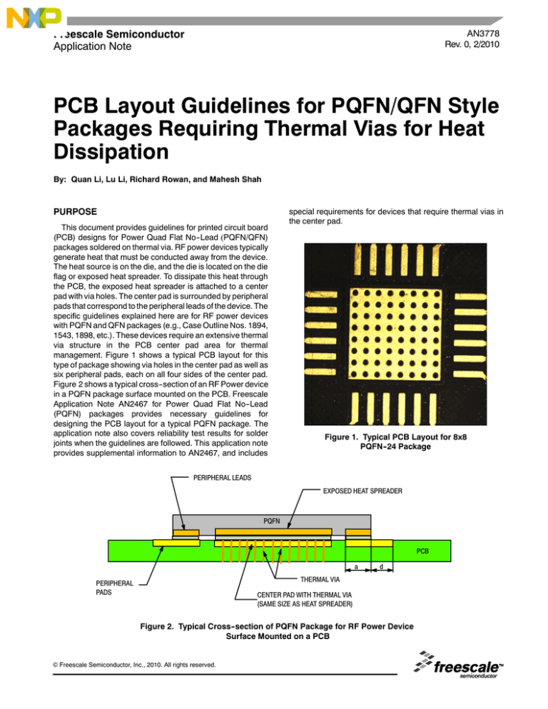
management. Figure 1 shows a typical PCB layout for this
type of package showing via holes in the center pad as well as
six peripheral pads, each on all four sides of the center pad.
Figure 2 shows a typical cross--section of an RF Power device
in a PQFN package surface mounted on the PCB. Freescale
Application Note AN2467 for Power Quad Flat No--Lead
(PQFN) packages provides necessary guidelines for
designing the PCB layout for a typical PQFN package. The
application note also covers reliability test results for solder
joints when the guidelines are followed. This application note
provides supplemental information to AN2467, and includes
special requirements for devices that require thermal vias in
the center pad.
Figure 1. Typical PCB Layout for 8x8
PQFN--24 Package
PERIPHERAL LEADS
EXPOSED HEAT SPREADER
PQFN
PCB
a
d
THERMAL VIA
PERIPHERAL
PADS
CENTER PAD WITH THERMAL VIA
(SAME SIZE AS HEAT SPREADER)
Figure 2. Typical Cross--section of PQFN Package for RF Power Device
Surface Mounted on a PCB
© Freescale Semiconductor, Inc., 2010. All rights reserved.
RF Application Information
Freescale Semiconductor
AN3778
1
BACKGROUND
Because of cost, the general trend for surface mount
devices (SMD) with via holes in the solder pad is to have
unfilled thermal via holes in the PCB. However, during solder
reflow, the liquid solder tends to wick into the thermal via holes,
resulting in solder volume loss between the exposed heat
spreader and center pad. When the solder solidifies, the
package is likely to be pulled down due to the large area of the
center pad which will cause the extra solder under the
peripheral leads of the package to spread out, forming
so--called solder balls (see Figures 3 and 4). The
solder--balling phenomenon has been well--known to occur
during solder reflow of PQFN/QFN--type leadless packages,
especially for center solder pads with extensive via holes. For
fine--pitch components, the solder--balling phenomena can
also result in solder bridging between two adjacent peripheral
pads.
design guidelines presented here are intended to minimize or
eliminate this.
Many factors during the PQFN package solder reflow
process affect solder balling, e.g., PCB layout, solder paste
screen--printing thickness, aperture size, solder alloy and
solder paste types, etc. For typical leaded SMT packages, the
extra solder volume under the leads tends to wet on the front
and back sides of the leads and create a fillet instead of
forming solder balls at the end of the leads or bridging between
leads. PQFN and QFN packages are leadless so they contain
no lead against which a fillet can be formed to take away
excess solder. However, the peripheral PCB pads can be
designed to accommodate any excess solder under the
peripheral leads, thus eliminating or reducing the probability
of solder--balling and bridging phenomena.
PCB PAD LAYOUT RECOMMENDATIONS
The PCB pad layout includes the design of both the center
pad and peripheral pads.
Recommendations from Application Note AN2467
a
d
e
LEAD
PERIPHERAL
PAD
b
b + 2e
e
Figure 5. Exposed Metal of Peripheral Pad Layout
Recommended in AN2467
Recommendations for peripheral pads from AN2467:
Figure 3. Solder Balling During Solder Reflow to
the PCB of PQFN Package
• Extension of the pad from the edge of the package
(d) -- 0.15 mm
• Width of the pad to be larger than lead nominal width on
each side (e) by 0.025 mm
• Minimum distance between two adjacent pads -- 0.15 mm
• Inside edge of the peripheral pad to be in line with inside
edge of the perpheral lead and between 0.15 and 0.25 mm
away from the center pad
Figure 4. Typical Cross--section of PQFN Package
Surface Mounted on PCB
The solder--balling phenomenon generally does not present
a reliability issue, but customers may be concerned that the
solder balls can become loose during transport, installation, or
operation and possibly create a short on the PCB trace. The
Because AN2467 does not provide much information on the
presence of via holes in the center pad and because concerns
of solder balling, additional experiments were performed to
define the minimum required values of pad dimension “d” to
address these concerns. Dimension “d” is important for
determining the pad extension needed to accommodate the
excessive solder during solder reflow. Based on an internal
evaluation using an 8x8 24--lead PQFN package, PCB pad
layout guidelines are provided for customers to facilitate the
design of the PCBs. These recommendations are provided as
a guide and may require some refinement for a specific
application or process. They are applicable for use with both
Sn--Pb eutectic and Pb--free solder alloys.
AN3778
2
RF Application Information
Freescale Semiconductor
BOARD MOUNTING EVALUATION
In general, the center pad with the thermal via should be the
same size as the maximum dimension of the exposed heat
spreader of the PQFN package. This helps the device to
self--center and provides the maximum number of via holes in
the pad. Another major consideration is the via pattern. The
via holes should be designed to minimize the thermal
resistance of the PCB. Before determining the via hole design,
an analysis of the PCB assembly stack should be conducted
to determine whether the device can operate within the
acceptable limits for junction temperature and whether the
PCB and the solder joint temperatures are within the
acceptable limits for the materials selected.
A Design of Experiment (DOE) was conducted with
dimension “d” as one of the parameters. In addition, the solder
joint material (Sn--Pb--Ag or Sn62, as well as Pb--free solder
alloy SAC305) was included as one of the parameters. Two
different stencil thicknesses for solder paste printing were also
used in the DOE. The full matrix is shown in Table 1.
Sample size in the DOE was five units per cell. The daisy
chain test board was designed for 8x8 PQFN--24 package
surface mount evaluation (see Figure 6). There was no die in
the test unit. The peripheral leads of the package were
internally connected (see Figure 7) by pad to pad wire bonds.
After the packages were surface mounted on the test boards,
six peripheral leads on each side were connected in series.
Each side of the PQFN package surface mounted on the test
board forms a separate loop with all of the solder joints on that
side forming series resistors (see Figure 8).
PCB parameters:
— via drill diameter = 12 mils, or 0.30 mm
— via pitch = 24 mils, or 0.60 mm
— copper plating in the via ~1 mil, or ~0.025 mm
— PCB thickness = 59 mils, or 1.50 mm
— PCB material = FR4
Table 1. Evaluation Matrix for Design of Experiment on the Pad Extension
Case #1
Stencil Thickness
(mil)
Solder Alloy
Dimension “d”
(mm)
4L--A
4
Sn62
0.00
4L--B
4
Sn62
0.20
4L--C
4
Sn62
0.40
4L--D
4
Sn62
0.60
4L--E
4
Sn62
0.80
6L--A
6
Sn62
0.00
6L--B
6
Sn62
0.20
6L--C
6
Sn62
0.40
6L--D
6
Sn62
0.60
6L--E
6
Sn62
0.80
4UL--A
4
SAC305
0.00
4UL--B
4
SAC305
0.20
4UL--C
4
SAC305
0.40
4UL--D
4
SAC305
0.60
4UL--E
4
SAC305
0.80
6UL--A
6
SAC305
0.00
6UL--B
6
SAC305
0.20
6UL--C
6
SAC305
0.40
6UL--D
6
SAC305
0.60
6UL--E
6
SAC305
0.80
AN3778
RF Application Information
Freescale Semiconductor
3
Figure 6. Daisy Chain Test Board for 8x8 PQFN--24 Package Solder Joint Evaluation
Figure 7. Internal Wire Bonds on Peripheral Leads (1.5 mil Au Wire) for Test Unit
AN3778
4
RF Application Information
Freescale Semiconductor
Figure 8. PQFN Unit Mounted on Test Board Creating Four Daisy Chain Resistors for
Six Solder Joints on Each Side
Assembly Reflow
Solder paste was screen--printed on the PCB with two
different thickness stencils (4 mils and 6 mils) and two different
solder pastes (Sn62 and SAC305). The devices were picked
and placed on top of the PCB pattern. The PCBs were then
reflowed in a 10--zone convection belt furnace in air
environment. The PCBs with Sn62 solder were reflowed using
a peak temperature of 218°C; the PCBs with SAC305
(Pb--free) were reflowed using a peak reflow temperature of
242°C. After the reflow and cleaning step, the solder joints
were examined by X--ray and visual inspection.
Solder Joints Visual and X--Ray Inspection
After the reflow, the solder joints were visually inspected
first. For cases with d < 0.20 mm, solder balling was visible on
most of the units evaluated. A typical case for Sn62 alloys is
shown in Figure 9. The solder--balling phenomenon for
Pb--free SAC305 solder is even more pronounced than that for
Sn62 solder (Figure 10). For cases with d > 0.40 mm, no solder
balling was observed for either solder material. Typical solder
joints are shown in Figure 11 (for Sn62 alloy) and Figure 12 (for
Pb--free SAC305 alloy).
Figure 9. Severe Solder Balling Observed for
Case 6L--A, d = 0.00 mm, Sn62 Solder
AN3778
RF Application Information
Freescale Semiconductor
5
Reliability Testing
Figure 10. Cross--section of Test Unit Showing
Solder Balling for Case 6UL--B,
d = 0.20 mm and SAC305 Solder
After reviewing the DOE results, the case with d = 0.4 mm
was chosen for a confirmation run with both Sn62 and Pb--free
SAC305 solder alloys. The confirmation run used 25 units for
each of the two cases. Again, the solder joints were visually
inspected. The results were satisfactory as expected.
The test boards with daisy chain solder joints were then
placed in a thermal cycling test. The temperature range for the
thermal cycling test was from --40°C to 125°C with 15--minute
dwell times at each extreme temperature. The duration of the
test was 2,000 cycles. Electrical resistance measurements for
each side of each test unit showed no solder joint failure.
Figure 13 shows the comparison of solder joint resistance of
the 50 thermal cycled boards with four non--thermal cycled
boards shown as zero cycle data. The electrical resistance
measurement revealed that there was no increase in the
solder joint resistance. Also on visual examination, no sign of
solder joint cracking was observed in either Sn62 or SAC305
solder alloy samples.
SOLDER JOINT RESISTANCE
0.085
RESISTANCE (Ω)
0.080
0.075
0.070
0.065
0.060
0.055
0.050
0.045
0 Cycle
1000 Cycles
1500 Cycles
2000 Cycles
Figure 13. Comparison of Electrical Resistance
Between Thermal Cycled and Non--thermal
Cycled Devices
Figure 11. No Solder Balling was Observed for
Case 6L--C, d = 0.40 mm, Sn62 Solder (Good Fillets
Formed Above the Extended Part of PCB Pads)
Figure 12. No Solder Balling was Observed for
Case 6UL--C, d = 0.40 mm, SAC305 Solder
AN3778
6
RF Application Information
Freescale Semiconductor
PAD LAYOUT RECOMMENDATIONS
Based on these evaluation results, Freescale recommends
using the following guidelines to determine the pad layout for
PQFN/QFN--style packages that require a large number of via
holes in the center pad:
1. Create symmetry of the leads and pads so that the device
can self--center on the pad layout.
2. Design the center pad so that it is equivalent to maximum
value of the exposed pad on the PQFN/QFN package.
3. Specify that the width of the peripheral pad is at least
0.05 mm larger than the nominal dimension of peripheral
leads.
4. Keep the inside edge of the peripheral pad to be in line with
the inside edge of the peripheral leads at the maximum
dimension.
5. Allow sufficient distance between the peripheral pads
(0.15 mm minimum recommended) to accommodate the
solder mask. This will prevent shorting between two pads
or between two leads.
6. Allow sufficient distance between the center pad and the
inside edge of the peripheral pads (0.15 mm minimum
recommended) to accommodate the solder mask and
prevent shorting between the center pad and peripheral
leads or between the peripheral pads or leads.
7. Specify that the peripheral pad extension past the package
(dimension “d” in Figure 5) is at least 40% of the peripheral
lead length nominal dimension.
These recommendations are provided as a guide. In some
instances compromises may have to be considered between
conflicting requirements.
Some PQFN style packages also have peripheral pads in
four corners of the package (e.g. Case 1543). The
recommendations given here for the peripheral pad layout are
also applicable to the corner pad layout.
The pad layout for the 8x8 PQFN--24 package (Case 1894)
using these guidelines is shown to create a solder joint free of
solder balling. This solder joint is also shown to survive the
normal reliability requirements of a typical RF power device.
The complete pad layout for the 8x8 PQFN--24 (Case 1894)
device using these guidelines is shown in Appendix A as
Figure A--1 Based on the guidelines derived from experiments
with 8x8 PQFN--24 (Case 1894), the pad layouts for 5x5
PQFN--16 (Case 1543) and 4x4 QFN--16 (Case 1898)
packages used for RF Power devices are shown in Figure A--2
and Figure A--3 respectively. As more products move into this
style of leadless packages, new guidelines will be added.
References
Freescale Application Note AN2467, Power Quad Flat Pack
No--Lead (PQFN).
AN3778
RF Application Information
Freescale Semiconductor
7
Appendix A
8.00
1.45
0.50
0.80
5.90
8.80
4.9 x 4.9 Solder
Pad with Thermal
Via Structure
Figure A--1. PCB Pads Layout for 8x8 PQFN--24 (Case 1894)
5.00
1.70
0.60
2.60
6.00
0.80
2.2 x 2.2 Solder
Pad with Thermal
Via Structure
Figure A--2. PCB Pad Layout for 5x5 PQFN--16 (Case 1543)
4.00
0.70
0.40
3.00
4.40
0.65
2.5 x 2.5 Solder
Pad with Thermal
Via Structure
Figure A--3. PCB Pad Layout for 4x4 QFN--16 (Case 1898)
AN3778
8
RF Application Information
Freescale Semiconductor
How to Reach Us:
Home Page:
www.freescale.com
Web Support:
http://www.freescale.com/support
USA/Europe or Locations Not Listed:
Freescale Semiconductor, Inc.
Technical Information Center, EL516
2100 East Elliot Road
Tempe, Arizona 85284
1--800--521--6274 or +1--480--768--2130
www.freescale.com/support
Europe, Middle East, and Africa:
Freescale Halbleiter Deutschland GmbH
Technical Information Center
Schatzbogen 7
81829 Muenchen, Germany
+44 1296 380 456 (English)
+46 8 52200080 (English)
+49 89 92103 559 (German)
+33 1 69 35 48 48 (French)
www.freescale.com/support
Japan:
Freescale Semiconductor Japan Ltd.
Headquarters
ARCO Tower 15F
1--8--1, Shimo--Meguro, Meguro--ku,
Tokyo 153--0064
Japan
0120 191014 or +81 3 5437 9125
support.japan@freescale.com
Asia/Pacific:
Freescale Semiconductor China Ltd.
Exchange Building 23F
No. 118 Jianguo Road
Chaoyang District
Beijing 100022
China
+86 10 5879 8000
support.asia@freescale.com
For Literature Requests Only:
Freescale Semiconductor Literature Distribution Center
1--800--441--2447 or +1--303--675--2140
Fax: +1--303--675--2150
LDCForFreescaleSemiconductor@hibbertgroup.com
Information in this document is provided solely to enable system and software
implementers to use Freescale Semiconductor products. There are no express or
implied copyright licenses granted hereunder to design or fabricate any integrated
circuits or integrated circuits based on the information in this document.
Freescale Semiconductor reserves the right to make changes without further notice to
any products herein. Freescale Semiconductor makes no warranty, representation or
guarantee regarding the suitability of its products for any particular purpose, nor does
Freescale Semiconductor assume any liability arising out of the application or use of
any product or circuit, and specifically disclaims any and all liability, including without
limitation consequential or incidental damages. “Typical” parameters that may be
provided in Freescale Semiconductor data sheets and/or specifications can and do
vary in different applications and actual performance may vary over time. All operating
parameters, including “Typicals”, must be validated for each customer application by
customer’s technical experts. Freescale Semiconductor does not convey any license
under its patent rights nor the rights of others. Freescale Semiconductor products are
not designed, intended, or authorized for use as components in systems intended for
surgical implant into the body, or other applications intended to support or sustain life,
or for any other application in which the failure of the Freescale Semiconductor product
could create a situation where personal injury or death may occur. Should Buyer
purchase or use Freescale Semiconductor products for any such unintended or
unauthorized application, Buyer shall indemnify and hold Freescale Semiconductor
and its officers, employees, subsidiaries, affiliates, and distributors harmless against all
claims, costs, damages, and expenses, and reasonable attorney fees arising out of,
directly or indirectly, any claim of personal injury or death associated with such
unintended or unauthorized use, even if such claim alleges that Freescale
Semiconductor was negligent regarding the design or manufacture of the part.
Freescalet and the Freescale logo are trademarks of Freescale Semiconductor, Inc.
All other product or service names are the property of their respective owners.
© Freescale Semiconductor, Inc. 2010. All rights reserved.
AN3778
RFAN3778
Application Information
Rev. 0, 2/2010
Freescale
Semiconductor
9

