Depletion-Enhancement CMOS Low Power Three
advertisement

IEEE JOURNAL
OF SOLID-STATE
CIRCUITS,
VOL
609
SC-20, NO 2, APRIL 1985
Depletion/Enhancement
CMOS For a
Low Power Family of Three-Valued
Logic Circuits
ALEX HEUNG
AND H. T. MOUFTAH,
SENIOR MEMBER, IEEE
4t
4<
INTRODUCTION
Depletlon-Type
p-channel:
Enhancement–Type
p-channel
:
T
HE
complementary
metal-oxide
semiconductor
(CMOS) family of integrated circuits has been used by
several authors in the realization
of three-valued
logic
circuits [1]–[8]. In all previous designs, these authors have
used voltage power supplies higher than the threshold
voltage of the p- and n-channel MOS transistors. In most
cases, this has resulted in high power consumption
in the
circuits. Recently, a new family of three-valued
CMOS
circuits that is not restricted to the use of power supplies at
the above threshold voltages has been reported [9] and
applied to the design of an all-CMOS ternary computer
[10]. ‘The new design [9], [10] reduces power consumption
in the circuits. In order to ‘further reduce the power consumption as well as increase the speed of these circuits, a
new design that does not use resistors at all is needed. Such
a design. would be extremely useful in the VLSI implementation of three-valued
digital systems. This paper is an
attempt to respond to this need, consolidating
ideas initially presented at ISMVL-84 [11].
In this paper, the design of a new family of ternary logic
circuits based on the use of depletion enhancement
complementary
metal-oxide-semiconductor
(DECMOS)
integrated circuits is presented. The circuits use two power
supplies each below the transistors’ threshold voltage and
do not require resistors. The circuit design of basic ternary
operators (inverters, NAND, NOR) is described. An example of the use of these basic ternary operators as building
blocks in the design of a ternary full adder is also presented.
Manuscript received March 30, 1984; rewsed September 6, 1984. Tlm
work was supported by the Natural Sciences and Engineering Research
Councd of Canada Grant A1056.
The au~hors are with Queen’s University, Kingston. Ontario. Canada
K7L 3N6
0018-9200/85
:
Legend:
+lV
I.
Depletion-Type
n-channel
Enhancement-Type
n-channel:
Abstract —A new family of ternary logic circuits that uses both depletion and enhancement types of complementary metal-oxide semiconductor
(CMOS) transistors is presented. These circuits use two power supplies
each Ibelow the transistor’s threshold voltages and do not include resistors.
Circuit designs of basic ternary operators (inverters, NAND, NOR) are
described. These basic ternary operators can be used as building blocks in
the VLSI implementation of three-valued digital systems. An example of
the design of a ternary full adder using this family of logic circuits is also
presented.
Cll
?
z
b
Co
c
Q3
I
Q4
-Iv
=
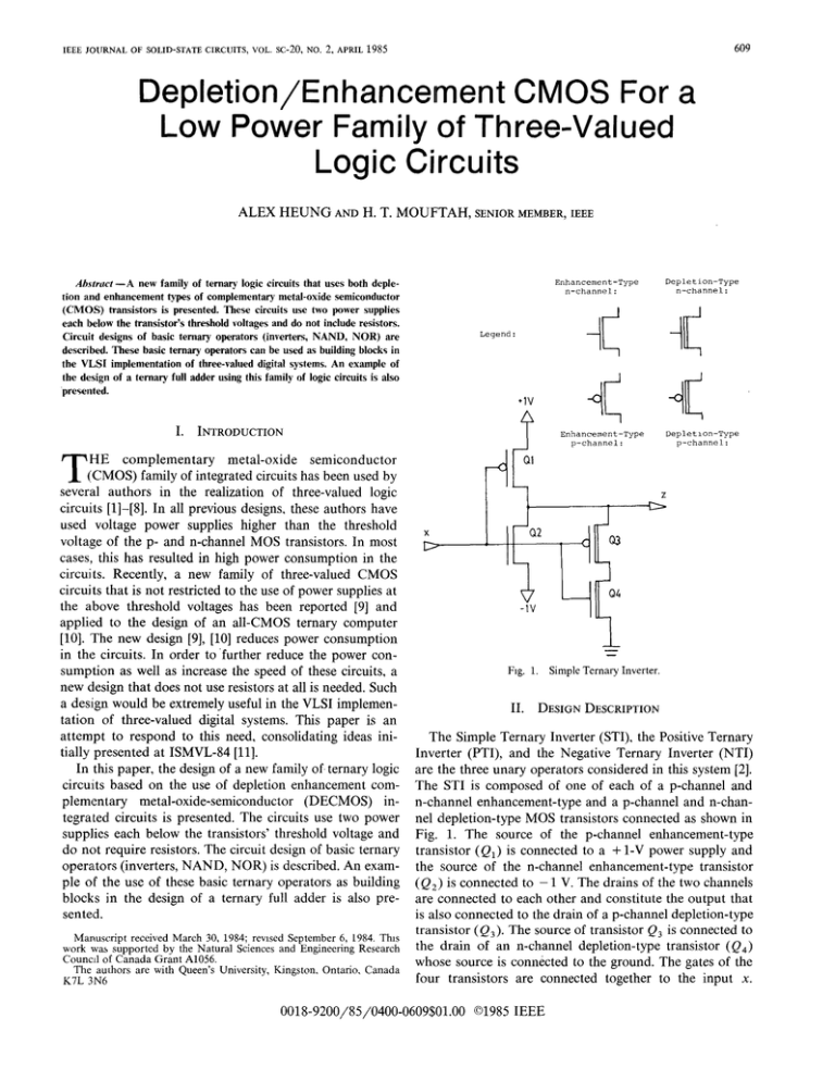
Fig. 1.
II.
Simple Ternary Inverter.
DESIGN DESCRIPTION
The Simple Ternary Inverter (STI), the Positive Ternary
Inverter (PTI), and the Negative Ternary Inverter (NTI)
are the three unary operators considered in this system [2].
The STI is composed of one of each of a p-channel and
n-channel enhancement-type
and a p-channel and n-channel depletion-type
MOS transistors connected as shown in
Fig. 1. The source of the p-channel
enhancement-type
transistor (Ql) is connected to a + 1-V power supply and
the source of the n-channel enhancement-type
transistor
(Qz) is connected to – 1 V. The drains of the two channels
are connected to each other and constitute the output that
is also connected to the drain of a p-channel depletion-type
transistor ( Q3 ). The source of transistor Q3 is connected to
the drain of an n-channel depletion-type
transistor (Qg)
whose source is connected to the ground. The gates of the
four transistors
are connected together to the input x.
/0400-0609$01.00
~1985 IEEE
610
IEEE JOURNAL
OF SOLID-STATE
CIRCUITS,
VOL.
SC-20, NO. 2,
APRIL
1985
+lV
All
Q3
Q1
+lV
x
111-
Flg
2,
AL
“
+,”
z
Q1
Q4
Q2
Q5
t
L
=
Fig. 3.
Positive Ternary Inverter
*.lV
Negative Ternary Inverter
TABLE I
DECMOS
POWER
CONSUMPTION,
rise
Gate
consumption
T
Power
STI
9.02
PTI
NTI
TNAND
TNOR
-1+0
pw
RISE
FALL
TIME
time
fall
0.1
10ns
AND
1+0
-1+1
1
time
0
+-1
1
+-1
10ns
18ns
--
70ns
--
--
13ns
--
15ns
--
--
70ns
5ns
10ns
13ns
15.00
pw
-.
15,00
pw
--
11.00
pw
15ns
25ns
25ns
25ns
2ons
25ns
18.00
PW
15ns
40ns
55ns
25ns
15ns
15ns
DECMOS
TABLE II
NOISE MARGIN CHARACTERISTICS
t
7
Noise
Margin
Gate
1+0
0+1
0
--1
1
.-1
-1.1
--
0.4V
0.4V
0.4V
0.45V
PTI
--
--
--
--
O.lv
0.45V
NT I
--
--
--
.-
0.45V
O.lv
0.4V
0.3V
0.4V
0.4V
--
--
0.3V
0.4V
0.35V
0.35V
--
--
ST I
TNAND
TNOR
Following one of many possible conventions, we shall label
the lower, middle, and upper levels logic – 1, 0, and 1,
respectively. Thus the STI is defined by [1], [2]
~o=—x
-1.0
the following
--
relationship
V<
must be satisfied:
VT<2V
(2)
O<l’’-P<V
(3)
(1)
where the minus sign represents arithmetic negation.
If the input x is at the high level (logic 1), transistor QI
will be off while transistor Q? will be on. At the same time,
Q3 will be off even though QA will be on which will keep
the output on the low level (logic – 1). The output will be
at logic 1 if the input x is at logic – 1 because in this case
QI and Q3 are on but Qz and Qq are off. However, if the
input x is at the intermediate level (logic O), both enhancement-type transistors QI and Qz will be off but depletiontype transistors Q~ and QA will be on which will force the
output to be at the ground voltage level (logic O).
Note that, for proper operation of the above STI circuit
where + V is the value of the power supply and V= is the
threshold voltage of the p-channel and/or
n-channel enhancement
MOS transistors, while VP is the pinchoff voltage of the p-channel and/or n-channel depletion devices.
The Positive Ternary Inverter uses five transistors connected as shown in Fig. 2. The source of a p-channel
depletion-type
transistor ( Ql) is connected to the ground
and the source of an n-channel enhancement-type
transistor ( Qz ) is connected to a – 1-V power supply. The
drains of the two channels are connected to each other and
the gate of a third transistor (Q3 ) of the n-channel depletion-type. The source of Qq is connected to + 1 V while its
drain is connected to the source of a fourth transistor (Qo)
HEUNG
AND
MOUFTAH:
CMOS FOR A FAMILY
OF THREE-VALVED
LOGIC
+Iv
+Iv
A
611
CIRCUITS
transistors Q2, Q4, and Q5 are on forcing the output to be
at logic – 1. However, the output will be at logic 1 if the
input is at logic —1 because transistors Q ~ and Q3 are on
while transistors Qz, Q4, and Q5 are all off.
The function of the PTI and NTI can be defined by
Q3
—
x’ =
&=———
I
i,
{ —x,
ifx=O
ifx#O
(4)
Q4
L
where i takes the value of 1 for the PTI and – 1 for the
NTI operator.
The ternary NAND and ternary NOR are two multiple
entry operators used in this system [2]. The functions of the
two-entry ternary NAND and ternary NOR are defined by
the following two equations, respectively,
1+
=
IQ8
Fig. 4
Ternary NAND
gate.
XAYO=min(X,
Y)O
(5)
XV YO=max(X,
Y)O.
(6)
*1V
-J
4
Q1
&——
u
IL—
o
3
i
Q2
-1
-Iv
,
z
\
Q6
-Iv
Fig. 5.
Ternary NOR gate.
of the p-channel depletion-type.
The drain of Q4 is connected to the drain of an n-channel enhancement-type
transistor
(Q5) and constitutes
the output of this PTI
circuit. The source of Q5 is connected to – 1 V and its gate
as well as the gates of transistors
Ql, Q2, and Q4 are
connected to the input x.
If the input x is at logic 1, transistor QI will be off while
transistor Q2 will be on, making point A – 1 V which will
force transistor Q3 to be off. At the same time transistor
Q. will be off while transistor Q5 will be on. Thus the
output will be at logic – 1. However, if the input is at logic
– 1 transistors Ql, Q3, and Q4 will be on while transistors
Q, and Q5 will be off forcing the output to be at logic 1.
The output will also beat logic 1 if the input x is at logic O
because the depletion-type
transistors Ql, Q3, and Q4 will
be on while the enhancement-type
transistors Q2 and Q5
will be off.
Similarly, the NTI circuit is designed with five transistors as shown in Fig. 3. Two enhancement-type
p-channel transistors
QI and Qq, two depletion-type
n-channel
transistors
Q2 and Q4, and one depletion-type
p-channel
transistor
Q5 are connected in a dual form of the PTI
circuit described above. In this case, when the input x is at
logic 1 or logic O transistors
QI and Q’s are off while
The circuits for the 2-input ternary NAND and ternary
NOR are shown in Figs. 4 and 5, respectively. They are
essentially the same as their binary counterpart
except for
the different power supplies and the additional depletion
mode devices connected to their inputs and centering the
output. In these two circuits, transistors QI – Q4 are of the
enhancement
type and transistors Q5 – Q8, which have the
same configuration
as QI – Q4 circuit, are of the depletion
type. The gates of transistors QI and Qt (enhancement)
and l,ransistors Q5 and Q7 (depletion) are connected as are
the gates of transistors
Q2 and Q4 (enhancement)
and
transistors QG and Qg (depletion). In these two circuits the
function of the depletion-type
transistors
is to pull the
output to the intermediate logic level (O V) when necessary.
The reader can apply the argument used in the STI case to
see that these circuits actually perform the desired logic
functions. For example, if inputs X and Y are logic O and 1
then the outputs of the ternary NAND and ternary NOR
will be logic O and – 1, respectively, because in both cases
transistors Ql, Qz, Qj, and Q6 are off while transistors Q4,
Qs, (?7, and Q8 are on.
It has to be noted here that (2) and (3) hold as a
condition
for proper operation also in the case of PTI,
NTI, ternary NAND, and ternary NOR circuits.
III.
The
performance
studied
sistor
using
of
the SPICE
PERFORMANCE
all
the
sizes are 5 pm x 5 pm. The
p-channel
– 1 amd
and
n-channel
+ 1 V,
above
circuits
2G Simulation
package.
threshold
enhancement-type
respectively,
while
for
has
been
All
tran-
voltages
of the
transistors
are
the depletion-type
transl[stors they are + 1 and – 1 V, respectively.
The vohage power supplies are as shown on all figures +1, O, and
– 1 V. The dc power consumption,
rise time, and fall time
for all of the above circuits are summarized in Table I. It
has been noted that notations
– 1 -+1 and 1 -+ – 1, on
Table I, are the 10–90-percent
and the 90–10-percent
612
IEEE JOURNAL
OF SOLID-STATE
CIRCUITS,
8,
“
~’>
id
,/”
SC-20, NO. 2, APRIL 1985
VOL.
/“”
4
q
. J(a)
!
“WA’”’’”’”’”
%1
.,
?i
.
\
\
///’”
+
:~
Vo”T
\,,—
\
. /“”
/“”
8
7
1/
I
-1.00
-o.&o
-0.s4
-0.40
-0.20
0.00
0.20
0.40
___.._.__-..__\
,,,,L,:,
: ~–—
t
5+-
,.
,“
?j.
/
+
//”
1
\
\
,< ~+-
~—+——
-0.!?0
O VUTS
,,/
/’”
~.W
Y -1.00
(xlOeXP
\
\,—%,
/“’”’”
;+
... .
‘
,.
/“
t
VIN
1.00
/’-’”
./
~+
O.ao
,/
3,
\
+
(b)
O.ao
-0.00
-0.40
-0. s0
0.00
0.20
0.40
0.80
1
0.s0
i.oo
VIN
(x.10exP O VOLTS I
:
-“
,,/
./”
%
&
...
8
es
[c)
q
?
./”
.,.,.?
?
s
7
4
-1.00
-0.eo
-0.s0
-0.40
-0.20
0.00
0.20
0.40
0.s0
O.eo
VIN
Fig. 6.
Static characteristics.
(a) STI. (b) PTI. (c) NTI.
1.00
(xlOeXP
O V04.TS 1
HEUNGANDMOUFTAH:
CMOS FOR AFAMILY
OF THt$EE-VALVEh
LOGIC
613
CIRCUITS
—....—
———-——
,’
-
vu”,
i?l
0
-.———
r-.+..LJ+...A.+.
~—+--=y
0.15
0.30
0.75
0.80
0.45
0.s0
1.05
1.20
1,ss
ixm
-_
(b)
V.*T
—0.15
0.30
-a SEcmqs)
._____
~+
8,
.
1.50
kloexp
O.ls
0.s0
0.45
-1
0.80
i.ss
1.05
TIE
1.s0
(xIoexp
-S SSCOM3S)
——
-U,,
-
Voln
..
.,
<;
(c)
\;
0.00
0.15
0.30
0.45
+
0.80
—.
~+-–+--+———+———+——
0.75
0.00
1.05
+-—-t---t---i
1.20
1.ss
TIHS
Fig. 7.
Dynamic
characteristics.
(a) STI. (b) PTI. (c) NTL
:.50
(KiO@XP -6 SECONDS)
IEEE JOURNAL OF SOLID-STATECIRCUITS, VOL.
614
mF
x
(a)
01-1
1-1o
TM
TM
Jk
TM
@
+.1”
+-IV
I
%
I
I
Fig. 10.
JK (.x) function
,r-––––Yl-–7
TM
I
I
I
I
I
I
I
J-1
JK
Jo
I
,
I
J,
1
I
I
I
I
[
I
[
I
I
l–––____
Fig. 9.
Ternary
J-J
T-gate
times fora2-V
swing while notations O~l. 1~0, Oa –1,
and – 1 ~ O are that of 1-V swing. The static and dynamic
characteristics
of the ternary inverter circuits are given in
Figs. 6 (a)–(c) and 7 (a)–(c), respectively. As can be seen
from the static characteristic
curves, the circuits have very
good noise margin of about 40 percent of the power
supplies in most cases (Table II). It has to be noted that the
rise and fall time of these circuits can be improved by
reducing the length to width (L/W)
ratio of the transistors used, at the expense of increased power consumption.
IV.
APPLICATION:
THE TERNARY
FULL ADDER
Based on the DECMOS ternary operator circuitry described above, it is possible to design any arbitrary ternary
digital system [2]. For illustration the design of a ternary
full adder is given below. In preparation,
the design of the
Jx. arithmetic circuit and the three-valued
T-gate are first
presented as they are used to construct the full adder. The
co
Ternary full adder
[12] is defined by
(b)
circuit. (a) Block diagram. (b’) Schematm
$
1
I
JK Arithmetic
‘6
as
%
t
x
~
1985
-1-10
a2
Fig. 8,
NO. 2, APRIL
3
~+lv
I
SC-20,
JK(X)=
(,_;’
ifx=k
ifx+k
(7)
where k can take the values of – 1, 0, or 1.
The JK arithmetic circuit is composed of an NTI, a PTI,
an STI, and a ternary NOR gate connected, as shown in
Fig. 8(a) in block diagram form and in Fig. 8(b) in schematic diagram form. In Fig. 8, it can be noticed, that the
depletion mode circuitry of the STI and the ternary NOR
has been omitted since their inputs and consequently their
output are never at logic O. This further reduces the complexity of the system.
The design of the T-gate circuit is based on the .J~
arithmetic
circuit described above. The function of the
T-gate [13] is described by
~(.h>y27h;x)=y,
(8)
where i will equal 1 if x takes the value of – 1.2 if x is O,
and 3 if x is 1.
The block diagram of the T-gate is shown in Fig. 9. It is
composed
of a JK arithmetic circuit and three ternary
switches (TS). Each TS consists of one p-channel and one
n-channel enhancement-type
transistor. The source of the
p-channel is connected to the drain of the n-channel and
vice versa. A control signal C is required for proper switch
operation.
This signal controls the n-channel directly and
the p-channel is controlled by C 0. Both channels are biased
on or off simultaneously
by the control signal C. When C
is equal to the high level ( + 1 V) the switch will be on, and
when C is equal to the low level ( – 1 V) the switch will be
off. The J _ ~, .1O,and .JI signals are connected to C of the
TS that has input yl, y2, and yq, respectively. The value of
x determines which TS will be on and, eventually, which
signal
( Y1,
Y2 or Y3) will be displayed
at the output.
A ternary full adder has been designed using DECMOS
HEUNG
AND
MOUFTAH:
CMOS FOR A FAMILY
OF THREE-VALVED
LOGIC
TABLE III
TRIJTH
TABLE
OF TERNARY
ADDER
Ci
s
co
-1
0
-1
1
-1
x
Y
-1
-1
-1
-1
0
-1
1
-1
FULL
-1
0
-1
0
0
-1
0
-1
0
1
0
0
-1
1
-1
-1
0
-1
1
0
0
0
-1
1
1
1
0
1
-1
0
-1
0
-1
0
-1
0
0
-1
1
0
0
0
0
-1
-1
0
-1
1
-1
0
0
0
0
0
0
0
1
1
0
0
1
-1
0
0
0
1
0
1
0
0
1
1
-1
1
1
-1
-1
-1
0
0
0
1
-1
0
1
-1
1
1
0
1
0
-1
0
0
1
0
0
1
0
1
0
1
-1
1
1
1
-1
1
0
1
1
0
-1
1
1
1
1
0
1
circuitry described above. The symmetric ternary number
system is used in this full adder. The truth table for the
sum and carry functions is given in Table HI. The full
adder is composed of fourteen T-gate circuits. However, a
large amount of circuitry can be saved by taking out the .J~
arithmetic circuits of all T-gates driven by a single trit and
to replace it by a single common .l~ arithmetic circuit
driving a number of ternary multiplexer
(TM), as shown
in Fig. 10. Each TM is composed of the set of three TS’S of
a T-gate. The complete ternary full adder has been simulated successfully on the computer using the SPICE 2G
simulation
package. The design parameters
are given in
Section HI above.
V.
supplies below the transistors
threshold voltage and the
exclusion
of resistors, it is possible to implement
this
circuitry in VLSI. This new family offers low power consumption, high speed, and comparable performance
to the
binary counterpart
circuitry.
0
-1
-1
615
CIRCUITS
CONCLUSIONS
A new family of ternary logic circuits based on both
depletion and enhancement
types of complementary
MOS
transistors (DECMOS) is shown to be useful in the design
of ternary digital systems. With the use of voltage power
[1] H. T. Mouftah
and L B. Jordan, “Integrated
circuits for ternary
logic,” in Proc. ISMVL- 74 (Morgantown), May 1974, pp. 285-302.
[2]
“Design of ternary COS\MOS
memory and sequential circtrits~” IEEE Trans. Computers, vol. C-26, pp. 281 –288, Mar. 1977.
[3] H. T. Mouftah, “A study on the implementation
of three-vafued
logic,” in Proc. ISM VL- 76 (Bloomington,
IL), May 1976, pp.
123-126.
[4] J. L. Huertas,
J. I. Acha, and J, M. Carmona,
“Design and
implementation
of tristables using CMOS integrated circuits,” IEE
J. Eleclron. Circuits Syst., vol. 1, no. 3, pp. 88-94, 1977.
of tristables using
[5] H. T. Mouftah, “Design and implementation
CMOS integrated circuits.” IEE J. Electron. Circuits Svst,.
., vol. 2.
no. 2, pp. 6~–62, 1978.
‘
[6] H. T. Mouftah and K. C. Smith, “Three-valued
CMOS cycling
gates,” Electron. Lett., vol. 14, pp. 36–37’, 1978.
[7] J. M. Carmona,
J. L. Huertas, and J, I. Acha, “Realization
of
three-vafued
CMOS cycling gates,” Electron. Lett., vol. 14, pp.
288-290, 1978.
[8] H. T. Koanantakool,
“Implementation
of ternary identity cell using
CMOS integrated circuits,” Electron, Lett., vol. 14, pp. 462-464,
1978.
[9] H. T, Mouftah
and K. C. Smith, “Injected
voltage low-power
(CMOS for three-valued logic, “ in IEE Proc., Part G, vol. 129, no. 6,
pp. 270–272, 1982.
[10] H. T. Mouftah, A, N. C. Heung, and L. M, C. Wong, “QTC-1: A
CMOS ternarv computer,” in Proc. ISMVL-84
(Winnive%
MA).
.“/
May, 1984, ppv 125-i32,
[11] Alex Heung and H, T. Mouftah, “ DECMOS—A
low power family
of three-vafued logic circuits for VLSI implementation,”
in Proc.
ISMVL-84
(Winnipeg, MA), May 1984, pp. 120-124.
[12] J. B. Rosser and A. R. Turquette, “Many-valued
Iogics,” Amsterdam, The Netherlands:
North Holland Publishing Co., 1952.
[13] C. Y, Lee and W. H, Chen. “ Several-vahred combinational
switching Circuits,” Trans. Amer.’Inst. Elec. Engrs., Vol. 75, 1956, No. 1,
pp. 278-283.
[14] H. T. Mouftah and K. C. Smith, “Design and Implementation
of
Three-valued
Logic systems with MOS Integrated Circuits,” IEE
Proceedings, Part G, Vol. 127, No. 4, 1980 pp. 165-168.
[15] K. C, Smith, “The Prospects for Multivalued Logic: A Technology
and Applications
View,” IEEE Trans. Comput., Vol. C-30, No. 9,
Sept. 1981, pm
~q. 61
---q–~~~
-. ..
[16] Z. G. Vram eslc, “Applications
and Scope of Multiple-Valued
LSI
Technology,” Proc. COMPCON 1981, San Francisco, pp. 213-216.
Alex N. C. Heung was born in Hong Kong on
July 1, 1961. He received the B. SC. (E. E.) degree
in computer engineering in 1983 from Queen’s
University at Kingston, Ontario, Canada. Presently he is finishing his M. SC. (E.E.) at Queen’s
University. The research topic is on the VLSI
implementation
of ternary logic systems.
Recently, he started working with Fitch Research Corporation
of Victoria,
British Columbia, Canada in the area of VLSI design and
implementation.
H. T. Mouftaft (S’74-M76-SM80) received the
B. SC. degree in electrical engineering, and the
M. SC. degree in computer science from the University of Alexandria, Alexandria, Egypt, in 1969
and 1972 respectively, and the Ph.D. degree in
electrical
engineering
from Laval University,
Quebec, Ontario, Canada, in 1975.
From 1969 to 1972 he was an instructor at the
University of Alexandria, Research and Teaching
Assistant at Laval University from 1973 to 1975,
Postdoctoral Fellow for the year 1975-76 at the
616
University
of Toronto, and Senior Digital Systems Engineer and then
Chlef Engineer at Adaptive Microelectronics
Ltd., Thornbdl, Ontario
from 1976 to 1977 From 1977 to 1979 he worked with the Data System
Planning Department
at Bell-Northern Research, Ottawa on several proJects related to Computer Commumcation Networks. In 1979 he Joined the
Department
of Electrical Engineering, Queen’s Umverslty at Kingston,
Ontario, Canada, where he is presently an Associate Professor, He has
IEEE JOURNAL
OF SOLID-STATE
CIRCUITS,
VOL
SC-’2(J, NO
~, APRtL
] 985
consulted for government and industry m the areas of Computer Communicatlons
and Digital Systems He holds a number of patents and
published a large number of technical articles in the area of Computer
Communications,
Digital Systems and Multiple-valued
Logic.
Dr. Mouftah is a Member of the Association of Professional Engineers
of Ontario, the Canadian
Society for Electrical Engineering,
and the
Canadian Association of University Teachers.

![VARIABLE, OPERATOR AND EXPRESSION [SET – 1]](http://s2.studylib.net/store/data/017977543_1-63cdff75b6f4ecbff2fecef218806221-300x300.png)

