MMA004AA
6-18GHz, 21dB Gain, 1.5dB NF
Low Noise Amplifier
Features
• 16dBm PSAT with 1.5dB NF and
21.5dB gain typical from 6-18GHz
• Gain flatness < +/-0.5dB
• Input and Output matched to 50Ω
• Self biased for simple biasing, small solution size and ease of manufacture
• +24dBm maximum input power rating
• 1.1mm x 1.36mm x 0.1mm die size
Applications
• Instrumentation
• Electronic warfare
• Microwave communications
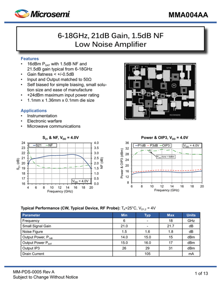
S21 & NF, VDD = 4.0V
Power & OIP3, VDD = 4.0V
Typical Performance (CW, Typical Device, RF Probe): TA=25°C, VD1,2 = 4V
Parameter
Min
Typ
Max
Units
Frequency
6
-
18
GHz
Small Signal Gain
21.0
-
21.7
dB
Noise Figure
1.5
1.6
1.8
dB
Output Power, P1dB
14.0
15.0
15
dBm
Output Power PSAT
15.0
16.0
17
dBm
26
29
31
dBm
Output IP3
Drain Current
MM-PDS-0005 Rev A
Subject to Change Without Notice
105
mA
1 of 13
MMA004AA
Table 1: Absolute Maximum Ratings, Not Simultaneous
Parameter
Rating
Units
Drain Voltage (VD)
+4.5
V
Input Power (PIN)
24
dBm
Channel Temperature (TC)
150
Operating Ambient Temperature (TA)
-55 to +85
°C
Storage Temperature
-65 to +150
°C
TBD (140 est)
°C/W
Thermal Resistance, Channel to Die Backside
1
°C
1
Caution, ESD
Sensitive Device
MTTF @ TC = 150°C > 10 hours
7
Table 2: Specifications (CW, 100% Test): TA = 25°C, VDD = 4V, IDD = 100mA
Parameter
Frequency
Min
Typ
Max
Units
Small Signal Gain
18GHz
18.0
21.0
-
dB
Output Power, P1dB
18GHz
-
1.8
2.3
dBm
RF Probe Measurement Set-Up With Reference Planes2
TO VDD
100nF CAPACITOR
TO GROUND
100nF CAPACITOR
TO GROUND
100pF CAPACITOR
TO GROUND
100pF CAPACITOR
TO GROUND
RFOUT
RFIN
50Ω TRANSMISSION LINE
MINIMIZE GAP
1mil Au wire used for
all bonds
2
Reference planes are the same for S-parameter files downloadable on www.microsemi.com/mmics
MM-PDS-0005 Rev A
Subject to Change Without Notice
2 of 13
MMA004AA
Typical Performance, RF Probe
VDD = 4V, IDD = 105, TA=25°C unless otherwise noted
S11 Over VDD
-10
-15
-20
-25
+25°C
2
4
6
8
10 12 14
Frequency (GHz)
16
S22 Over Temperature, VDD = 4.0V
S22 Over VDD
20
S22 Over Temperature, VDD = 3.3V
+85°C
18
S11 (dB)
VDD = 4.0V
-5
S11 Over Temperature, VDD = 4.0V
0
-30
S11 Over Temperature, VDD = 3.3V
MM-PDS-0005 Rev A
Subject to Change Without Notice
3 of 13
MMA004AA
Typical Performance, RF Probe
VDD = 4V, IDD = 105, TA=25°C unless otherwise noted
S21 Over VDD
S21 Over Temperature, VDD = 4.0V
NF Over VDD
NF Over Temperature, VDD = 3.3V
MM-PDS-0005 Rev A
Subject to Change Without Notice
NF Over Temperature, VDD = 4.0V
S21 Over Temperature, VDD = 3.3V
4 of 13
MMA004AA
Typical Performance, RF Probe
VDD = 4V, IDD = 105, TA=25°C unless otherwise noted
P1dB Over VDD
Power Sweep, VDD = 4.0V
OIP3 Over POUT/tone, VDD = 3.3V3
OIP3 Over POUT/tone, VDD = 4.0V3
3
Power Sweep, VDD = 3.3V
P3dB Over VDD
OIP3 over POUT/tone can be adjusted using VD1 and VD2
MM-PDS-0005 Rev A
Subject to Change Without Notice
5 of 13
MMA004AA
Typical Performance, RF Probe
VDD = 4V, IDD = 105, TA=25°C unless otherwise noted
Power & OIP3, VDD = 3.3V4
IMD Sweep, VDD = 3.3V4
4
S21 & NF, VDD = 3.3V
IMD Sweep, VDD = 4.0V4
OIP3 over POUT/tone can be adjusted using VD1 and VD2
MM-PDS-0005 Rev A
Subject to Change Without Notice
6 of 13
MMA004AA
Connectorized Test Fixture
With 2.92mm Connectors
VD1 Feedthru
0.1uF
VD2 Feedthru
100pF 100pF
0.1uF
1.000
0.950
MM-PDS-0005 Rev A
Subject to Change Without Notice
7 of 13
MMA004AA
Typical Performance, Connectorized Test Fixture
VDD = 4V, IDD = 105, TA=25°C unless otherwise noted
S11 Over Temperature
S22 Over Temperature
MM-PDS-0005 Rev A
Subject to Change Without Notice
P3dB Over Temperature
P1dB Over Temperature
NF Over Temperature
S21 Over Temperature
8 of 13
MMA004AA
Typical Performance, Connectorized Test Fixture
VDD = 4V, IDD = 105, TA=25°C unless otherwise noted
Power Sweep, -40°C
OIP3 Over Temperature, POUT/tone = 6dBm5
OIP3 Over Temperature, POUT/tone = 3dBm5
OIP3 Over Temperature, POUT/tone = 0dBm5
5
Power Sweep, +85°C
Power Sweep, +25°C
OIP3 over POUT/tone can be adjusted using VD1 and VD2
MM-PDS-0005 Rev A
Subject to Change Without Notice
9 of 13
MMA004AA
Typical Performance, Connectorized Test Fixture
VDD = 4V, IDD = 105, TA=25°C unless otherwise noted
IMD3 Sweep, -40°C6
IMD3 Sweep, +25°C6
IMD3 Sweep, +85°C6
-100
-120
-130
-140
-150
-160
-170
-180
VDD = 4.0V
-110
6.5GHz
00
10
-120
-130
-140
-150
-160
-180
6
7
8.0GHz
00
10
11
10
22
33
10
1044
10
Frequency (Hz)
22
33
10
1044
10
Frequency (Hz)
-100
VDD = 4.0V
-110
Phase Noise (dBc)
Phase Noise (dBc)
-100
11
10
55
10
66
10
1077
Phase Noise7, 9.5GHz
Phase Noise7, 8.0GHz
-170
Phase Noise7, 6.5GHz
Phase Noise (dBc)
55
10
66
10
1077
VDD = 4.0V
-110
-120
-130
-140
-150
-160
-170
-180
9.5GHz
00
10
11
10
22
33
10
1044
10
Frequency (Hz)
55
10
66
10
1077
OIP3 over POUT/tone can be adjusted using VD1 and VD2
Visit www.microsemi.com/mmics for application note on phase noise measurement at Microsemi
MM-PDS-0005 Rev A
Subject to Change Without Notice
10 of 13
MMA004AA
Typical Performance, Connectorized Test Fixture
VDD = 4V, IDD = 105, TA=25°C unless otherwise noted
Phase Noise8, 11.0GHz
-120
-130
-140
-150
-160
-170
-180
8
-100
VDD = 4.0V
-110
Phase Noise (dBc)
Phase Noise (dBc)
-100
Phase Noise8, 12.5GHz
11.0GHz
00
10
11
10
22
33
10
1044
10
Frequency (Hz)
55
10
66
10
1077
VDD = 4.0V
-110
-120
-130
-140
-150
-160
-170
-180
12.5GHz
00
10
11
10
22
33
10
1044
10
Frequency (Hz)
55
10
66
10
1077
Visit www.microsemi.com/mmics for application note on phase noise measurement at Microsemi
MM-PDS-0005 Rev A
Subject to Change Without Notice
11 of 13
MMA004AA
Chip layout showing pad locations.
All dimensions are in microns. Die thickness is 100 microns. Backside metal is gold, bond pad metal is gold.
Refer to Die Handling Application Note MM-APP-0001 (visit www.microsemi.com/mmics).
1115
965
589
3
1100
922
4
5
2
6
1
7
437
437
262
262
50
1172
1350
Table 3: Pad Descriptions
Pad #
Description
Pad Dimensions (µm)
1, 4, 7
Ground
100 x 100
2
RFIN, pad is AC coupled
100 x 150
3
VD1
100 x 100
5
VD2
100 x 100
6
RFOUT , pad is AC coupled
100 x 150
Biasing
MMA004AA is a self-biased device with positive supply. Apply VDD to pad 3 and 5.
VD1 and VD2 should be RF isolated from each other. Bias sequence does not matter.
MM-PDS-0005 Rev A
Subject to Change Without Notice
12 of 13
MMA004AA
Information contained in this document is proprietary to Microsem. This document may not be modified in any way without the express
written consent of Microsemi. Product processing does not necessarily include testing of all parameters. Microsemi reserves the right to
change the configuration and performance of the product and to discontinue product at any time.
Microsemi Corporate Headquarters
One Enterprise, Aliso Viejo CA 92656 USA
Within the USA: +1 (949) 380-6100
Sales: +1 (949) 380-6136
Fax: +1 (949) 215-4996
Microsemi Corporation (Nasdaq: MSCC) offers a comprehensive portfolio of semiconductor
and system solutions for communications, defense and security, aerospace, and industrial
markets. Products include high-performance and radiation-hardened analog mixed-signal
integrated circuits, FPGAs, SoCs, and ASICs; power management products; timing and
synchronization devices and precise time solutions, setting the world’s standard for time;
voice processing devices; RF solutions; discrete components; security technologies and
scalable anti-tamper products; Power-over-Ethernet ICs and midspans; as well as custom
design capabilities and services. Microsemi is headquartered in Aliso Viejo, Calif. and has
approximately 3,400 employees globally. Learn more at www.microsemi.com.
© 2014 Microsemi Corporation. All rights reserved. Microsemi and the Microsemi logo are trademarks of Microsemi Corporation. All other
trademarks and service marks are the property of their respective owners.
MM-PDS-0005 Rev A
Subject to Change Without Notice
13 of 13

![6.012 Microelectronic Devices and Circuits [ ]](http://s2.studylib.net/store/data/013591838_1-336ca0e62c7ed423de1069d825a1e4e1-300x300.png)
