HITFETâ BTS3408G
Smart Dual Lowside Power Switch
Data Sheet V1.0
Features
•
•
•
•
•
•
•
•
•
•
•
•
•
•
Logic Level Input
Compatible to 3V micro controllers
ESD protection
Thermal shutdown with auto restart
Overload protection
Short circuit protection
Over voltage protection
Open load detection (during Off)
Current limitation
Direct parallel control of the inputs
FREEZE functionality for multiplexing
General fault flag
Very low standby quiescent current
Switching frequencies up to 50kHz
Application
•
•
•
•
All kinds of resistive, inductive and capacitive loads in switching applications
µC compatible power switch for 12 V, 24 V and 42 V applications
Replaces electromechanical relays and discrete circuits
Line, stepper motor, lamp and relay driver
General Description
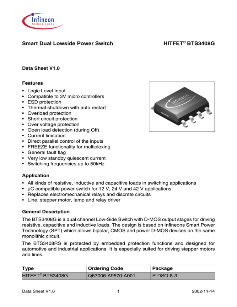
The BTS3408G is a dual channel Low-Side Switch with D-MOS output stages for driving
resistive, capacitive and inductive loads. The design is based on Infineons Smart Power
Technology (SPT) which allows bipolar, CMOS and power D-MOS devices on the same
monolithic circuit.
The BTS3408RS is protected by embedded protection functions and designed for
automotive and industrial applications. It is especially suited for driving stepper motors
and lines.
Type
â
HITFET BTS3408G
Data Sheet V1.0
Ordering Code
Package
Q67006-A9570-A001
P-DSO-8-3
1
2002-11-14
HITFETâ BTS3408G
Product Summary
Parameter
Symbol
Value
Unit
Supply voltage
VS
VDS
RDS(ON)
ID(lim)
ID(Nom)
EAS
4.5 - 60
V
60
V
550
mΩ
1
A
0.55
A
800
mJ
Continuous drain source voltage
On-state resistance
Current limitation
Nominal output current (individual channel)
Clamping energy
VS
Vbb
BTS 3408
Logic
Protection
Protection
and
Diagnosis
Control
Open Drain
Status
Feedback
Normal Function
Over Temp
Short Circuit
Open Load @ OFF
IN1
IN2
LOAD
FAULT
OUT1
Freeze
functionality
Output
Control
OUTPUT Stage
OUT2
ENA
GND
Figure 1
Block Diagram
1
Figure 2
VS
FAULT
8
2
IN1
OUT1
7
3
IN2
GND
6
4
ENA
OUT2
5
Pin Configuration
Data Sheet V1.0
2
2002-11-14
HITFETâ BTS3408G
Pin Definitions and Functions
Pin
Symbol
Function
1
FAULT
General Fault Flag; see Table 2 for operation mode.
2
IN1
Input 1; input of channel 1; has an internal pull down; TTL/
CMOS compatible input.
3
IN2
Input 2; input of channel 2; has an internal pull down; TTL/
CMOS compatible input.
4
ENA
Enable/Freeze; has an internal pull down; device is enabled
when voltage is higher then 1.2 Volts; if the voltage is below 1.7
Volts the output is freezed, input signals will be ignored; if the
voltage is above 2 Volts input signals will be output ; see
Table 1 for detailed information.
5
OUT2
Output 2; output of D-MOS stage 2.
6
GND
Ground.
7
OUT1
Output 1; output of D-MOS stage 1.
8
VS
Power supply.
Data Sheet V1.0
3
2002-11-14
HITFETâ BTS3408G
Circuit Description
Logic Supply
The logic is supplied with 4.5 up to 60 Volt by the VS pin. If VS falls below max. 4.5 Volts
the logic is shut down and the output stages are switched off.
Direct Inputs
ENA
The ENA/FREEZE input can be used to enable and/or to freeze the output control of the
IC or to cut off the complete IC.
By pulling the ENA input to low, i.e. applying a Voltage VENAL , the IC is in disable mode.
The power stages are switched off and the current consumption is reduced to IS(stby).
By applying a Voltage VENAFZ , the IC is in FREEZE mode. The output signals will remain
in their former state. All input signals will be ignored.
By pulling the input to high, the IC is in Enable mode. All input signals are output.
The ENA - pin has an internal pull-down.
IN1 / IN2
Each output is independently controlled via the respective input pin. The input pins are
high active. If the common enable pin is high, the individual input signals are output. The
input pins have an internal pull-down.
Table 1
Functional Table
VENA
Mode
≤0.8V
Disable X 1) X 1) X 1)
IN1 IN2 IN1(-1) IN2(-1) OUT1 OUT2 Comment
X 1)
L
L
all outputs OFF
L
L
L
L
former output state
1.2 .. 1.7V Freeze X 1) X 1) L
H
L
H
former output state
1.2 .. 1.7V Freeze X 1) X 1) H
L
H
L
former output state
1.2 .. 1.7V Freeze X 1) X 1) H
H
H
H
former output state
≥2.0V
Enable L
L
X 1)
X 1)
L
L
input is output
≥2.0V
Enable L
H
X 1)
X 1)
L
H
input is output
≥2.0V
Enable H
L
X 1)
X 1)
H
L
input is output
≥2.0V
Enable H
H
X 1)
X 1)
H
H
input is output
1.2 .. 1.7V Freeze X
1)
1)
X
1)
X = not relevant
Data Sheet V1.0
4
2002-11-14
HITFETâ BTS3408G
Power stages
Each output is protected by embedded protection functions. In the event of an overload
or short to supply, the current is internally limited. The current limit is set to ID(lim). If this
operation leads to an overtemperature condition, a second protection level (about 165
°C) will turn the effected output into a PWM-mode (selective thermal shutdown with
restart) to prevent critical chip temperatures. The temperature hysteresis is typically 10K.
Zener clamping is implemented to limit voltages at the power transistors when inductive
loads are switched off.
Diagnostic
The general FAULT pin is an open drain output. The FAULT pin is low active. It signals
fault conditions of any of the two output stages. By doing so, single and/or dual fault
conditions can be monitored. Single fault conditions can be assigned.
Table 2
Diagnostic Table
Operating Condition
ENA
INX
OUTX
FAULT
Standby
L
X 1)
OFF
H
Normal function
H
H
ON
H
Over temperature
H
H
OFF 2)
L
Open load / short to ground
H
L
OFF
L
1)
X = not relevant
2)
selective thermal shutdown for each channel at overtemperature
Fault Distinction
Open load / short to ground is recognized during OFF-state. Overtemperature as a result
of an overload or short to battery can only arise during ON-state. If there is only one fault
at a time, it is possible to distinguish which channel is affected with which fault.
.
Data Sheet V1.0
5
2002-11-14
HITFETâ BTS3408G
Absolute Maximum Ratings 1)
Tj = -40°C to 150°C , unless otherwise specified
Parameter
Symbol
Values
Unit Remarks
Supply Voltage
VS
VDS
VIN
IIN
VFault
Tj
Tstg
Ptot
ID(Nom)
+4.5 .. +60
V
–
-0.3 .. +60
V
–
-0.3 … +7
V
–
1
mA –
-0.3 … +7
V
Drain source voltage (OUT1, OUT2)
Input voltage (IN1, IN2, ENA)
Continuous input current VIN>7V
FAULT output voltage
Operating temperature range
Storage temperature range
Power dissipation (DC) 2)
Nominal load current 2)
one channel active
both channel active
-40 … +150 °C
-55 … +150 °C
–
0.88
W
–
A
VDS≤0.5V,
Tj≤150°C,
TA=85°C,
VIN=5V
800
mJ
ID=0.7A,
Tj(start)=25°C
0.55
0.45
Unclamped single pulse inductive energy EAS
one channel active
–
Electrostatic discharge voltage (Human
Body Model)
according to MIL STD 883D, method
3015.7 and EOS/ESD assn. standard
S5.1 - 1993
VESD
2000
V
–
DIN humidity category, DIN 40 040
–
E
–
–
IEC climatic category, DIN IEC 68-1
–
40/150/56
–
–
RthJS
RthJA
≤ 10
K/W –
≤ 185
≤ 142
K/W –
Thermal Resistance
Junction soldering point
Junction - ambient @ min. footprint
Junction - ambient @ 6cm² cooling area 2)
1)
Stresses above those listed here may cause permanent damage to the device. Exposure to absolute maximum
rating conditions for extended periods may affect device reliability.
2)
Device on epoxy pcb 40 mm × 40 mm × 1.5 mm with 6 cm2 copper area for pin 4 connection.
Data Sheet V1.0
6
2002-11-14
HITFETâ BTS3408G
Electrical Characteristics
VS = 4.5 to 18V; Tj = -40 to 150°C; unless otherwise specified
Parameter
Symbol
Limit Values
Unit Test Conditions
min. typ.
max.
4.5
–
60
V
–
1.5
4
mA ENA=High,
OUT1=OUT2=On
–
16
µA
ENA=Low
–
75
V
ID = 1 mA
Output leakage current 2)
VDS(AZ) 60
IDSS
–
1
5
µA
ENA=Low,
IN=Low,
VDS = 60 V
Output pull down current
IPD(OL) 50
100
200
µA
ENA=High,
IN=Low,
VDS = 42 V
On-state resistance
RDS(on)
Power supply
Supply voltage
Supply current in enable mode
VS
IS(ON)
Supply current in standby mode 1) IS(stby) –
–
Power outputs
Drain source clamp voltage
Tj = 25 °C
Tj = 150 °C
mΩ ID = 0.2 A,
VS = 5 V
–
–
480
800
550
1000
ID(lim)
Turn-on time IN=High to 90% ID: ton
1
1.5
2
A
–
–
2
8
µs
Turn-off time IN=Low to 10% ID: ton
–
2
8
µs
RL=2kΩ,
VBB=12V,VS=5V
RL=2kΩ,
VBB=12V,VS=5V
Current limit
Digital inputs (IN1, IN2, ENA)
Input ’Low’ voltage
IN1, IN2:
ENA:
ENA voltage for ’FREEZE’
functionality
Data Sheet V1.0
-0.3 –
VINL
VENAL -0.3 –
VENAFZ 1.2 –
7
V
–
V
–
0.8
0.8
1.7
2002-11-14
HITFETâ BTS3408G
Electrical Characteristics (cont’d)
VS = 4.5 to 18V; Tj = -40 to 150°C; unless otherwise specified
Parameter
Input ’High’ voltage
IN1, IN2:
ENA:
Input voltage hysteresis
Input pull down current
IN1, IN2:
ENA:
Symbol
Limit Values
min. typ.
Unit Test Conditions
max.
V
VINH 2.0
VENAH 2.0
VINhys –
–
–
–
–
300
–
IINPD 20
IENAPD 20
50
50
100
100
VFLTL
–
0.4
–
mV –
µA
–
V
IFLTL=1.6mA,
Digital Output (FAULT)
Output ’Low’ voltage
–
Diagnostic Functions
Open load / short to ground
detection voltage
VDS(OL) 0.5*VS 0.7*VS 0.9*VS V
Fault filter time for open load
tfilter(OL) 30
100
200
µs
VS=5V
Thermal overload trip
temperature
Tjt
150
165
180
°C
–
Thermal hysteresis
∆Tjt
–
10
–
Κ
–
mJ
ID=0.7 A
–
Protection Functions 3)
Unclamped single pulse inductive EAS
energy
one channel active,Tj(start)=25°C
both channel active,Tj(start)=25°C
one channel active,Tj(start)=150°C
both channel active,Tj(start)=150°C
800
550
240
240
1)
See also diagram 4 on page 14.
2)
See also diagram 5 on page 14.
3)
Integrated protection functions are designed to prevent IC destruction under fault conditions described in the
data sheet. Fault conditions are considered as "outside" normal operating range. Protection functions are not
designed for continuous repetitive operation.
Data Sheet V1.0
8
2002-11-14
HITFETâ BTS3408G
EMC-Characteristics
The following EMC-Characteristics outline the behavior of typical devices. They are not
part of any production test.
Table 3
Test Conditions
Parameter
Symbol
Value
Unit
Remark
Temperature
TA
23 ±5
°C
–
Supply Voltage
VBB
13.5
V
–
Input Voltage (ENA, IN1, IN2)
VINx
5
V
–
Load
RL1 , RL2
27
Ω
ohmic
Operation mode
PWM
DC
–
–
–
–
fINx=100Hz, D=0.5
ON / OFF
DUT specific
all tests with ENA=HIGH
Fast electrical transients
acc. to ISO 7637
Test Result
Test1)
Pulse
Max.
Test
Level
VS and OUTx
stressed
ON
1)
OUTx stressed
OFF
ON
OFF
Pulse Cycle Time
and Generator
Impedance
1
-200V
E(-120V) E(-120V)
C
C
500ms ; 10Ω
2
+200V
E(+120V E(+120V
C
C
500ms ; 10Ω
3a
-200V
C
C
C
C
100ms ; 10Ω
3b
+200V
C
C
C
C
100ms ; 10Ω
4
-7V
C
C
C
C
0.01Ω
5
175V
E(50V)
E(65V)
E(70V)
E(75V)
400ms ; 2Ω
The test pulses are applied at VBB
Definition of functional status
Class
Content
C
All functions of the device are performed as designed after exposure to
disturbance.
E
One or more function of a device does not perform as designed after
exposure and can not be returned to proper operation without repairing
or replacing the device. The value after the character shows the limit.
Data Sheet V1.0
9
2002-11-14
HITFETâ BTS3408G
Figure 3
VBB
Test circuit for ISO pulse
PULSE
stress also for VS
13.5V
3408 VS
RL1
RL2
FAULT
OUT1
IN1
IN2
OUT2
ENA GND
Data Sheet V1.0
10
2002-11-14
HITFETâ BTS3408G
Conducted Emissions
Conducted Susceptibility
Acc. IEC 61967-4 (1Ω/150Ω method)
Acc. I47A/658/CD IEC 62132-4 (Direct
Power Injection)
Typ. OUTx Emissions at PWM-mode
with 150Ω-matching network
Direct Power Injection: Forward Power
CW
100
Failure Criteria: Amplitude or frequency
variation max. 10% at OUT
Noise
OUT1
OUT2
150ohm Class1
150ohm Class6
90
80
70
60
dBµV
50
Typ. OUTx Susceptibility at DC-ON/OFF
and at PWM
150Ω / 8-H
40
30
20
40
150Ω / 13-N
10
35
0
-10
30
-20
0,1
1
10
100
25
1000
dBm
f / MHz
Limit
OUT2, ON
OUT2, OFF
OUT2, PWM
20
15
Figure 4
10
Test circuit for conducted
emission 1)
5
0
1
VBB
10
100
1000
f / MHz
Figure 5
VBB
5V
3408 VS
FAULT
OUT1
IN1
IN2
OUT2
ENA GND
Test circuit for conducted
susceptibility 2)
RL1
RL2
5V
B
A
N
B
A
N
150Ω
Ω-Network
3408 VS
150Ω
Ω-Network
FAULT
OUT1
IN1
IN2
OUT2
ENA GND
RL1
RL2
HF
HF
2)
1)
For defined decoupling and high reproducibility a
defined choke (5µH at 1 MHz) is inserted between
Vbb and Out-Pin.
Data Sheet V1.0
11
Broadband Artificial Network (short BAN) consists
of the same choke (5µH at 1 MHz) and the same
150ohm-matching network as for emission
measurement for defined decoupling and high
reproducibility.
2002-11-14
HITFETâ BTS3408G
Terms
VS
IS
VS
IFLT
FAULT
VFLT
IIN1
ID1
IN1
VIN1
OUT1
IIN2
VDS1
IN2
ID2
VIN2 IENA
Figure 6
OUT2
ENA
VENA
VBB
VDS2
GND
Figure 8
Input circuit
(ESD protection)
Application Circuit
VBB
uC Vcc
ESD zener diodes are not designed for DC
current.
Figure 7
INT
Inductive and over
voltage output clamp
Px.1
LOAD
Drain
VAZ
3408 VS
FAULT
IN1
OUT1
Px.2
IN2
Py.1
OUT2
ENA
GND
line
GND
VDS
Power
DMOS
Source
ID
Data Sheet V1.0
12
2002-11-14
HITFETâ BTS3408G
Timing diagrams
Characteristics
Figure 9
1. Max. allowable Power Dissipation
Ptot = f(Tamb)
Switching a resistive load
ENA
1
INx
P
VDSx
to t
6cm ²
0W
,8
m in . fo o tp rin t
t
0.9*ID
IDx
0 ,6
0.1*ID
ton
Figure 10
toff
t
0 ,4
Switching an inductive
load
0 ,2
ENA
INx
0
-5 0
VDS(AZ)
VDSx
-2 5
0
25
50
75
1 0 0 1°C
25 150
T
VBB
am b
2. On-state Resistance RON = f(Tj);
ID = 0.2 A; VS = 5 V
t
IDx
1000
R
ON
9 0Ω0
m
t
800
Figure 11
Short circuit
m a x.
700
ENA
600
INx
500
typ .
400
IDx
300
t
ϑjx
200
thermal hysteresis
100
t
0
FAULT
-5 0 -2 5
0
25
50
75
1 0 0 1°C
25 150
T
Data Sheet V1.0
13
j
2002-11-14
HITFETâ BTS3408G
3. Typ. Short Circuit Current
5. Typ. Output leakage current
ID(lim) = f(Tj)
IDSS = f(Tj);VS = 18 V; VDS = 60 V
2
2
I D (lim )
I DSS
typ .
1µ,6
A
1A,5
ty p .
1 ,2
1
0 ,8
0 ,5
0 ,4
0
0
-5 0
-2 5
0
25
50
75
1 0 0 1°C
25 150
T
-5 0
-2 5
0
25
50
75
1 0 0 1°C
25 150
T
j
j
4. Typ. Supply current in Standby mode
IS(stby) = f(Tj);VS = 5 V
10
I S (s tb y)
µ 8A
typ .
6
4
2
0
-5 0
-2 5
0
25
50
75
1 0 0 1°C
25 150
T
Data Sheet V1.0
j
14
2002-11-14
HITFETâ BTS3408G
Package Outlines
GPS05560
P-DSO-8-3
(Small Outline Transistor)
Sorts of Packing
Package outlines for tubes, trays etc. are contained in our
Data Book “Package Information”
SMD = Surface Mounted Device
Data Sheet V1.0
15
Dimensions in mm
2002-11-14
HITFETâ BTS3408G
Published by
Infineon Technologies AG,
Bereichs Kommunikation
St.-Martin-Strasse 76,
D-81541 München
© Infineon Technologies AG 1999
All Rights Reserved.
Attention please!
The information herein is given to describe certain components and shall not be
considered as warranted characteristics.
Terms of delivery and rights to technical change reserved.
We hereby disclaim any and all warranties, including but not limited to warranties of
non-infringement, regarding circuits, descriptions and charts stated herein.
Infineon Technologies is an approved CECC manufacturer.
Information
For further information on technology, delivery terms and conditions and prices please
contact your nearest Infineon Tech-nologies Office in Germany or our Infineon
Technologies Representatives worldwide (see address list).
Warnings
Due to technical requirements components may contain dangerous substances. For
information on the types in question please contact your nearest Infineon Technologies
Office.
Infineon Technologies Components may only be used in life-support devices or systems
with the express written approval of Infineon Technologies, if a failure of such
components can reasonably be expected to cause the failure of that life-support device
or system, or to affect the safety or effectiveness of that device or system. Life support
devices or systems are in-tended to be implanted in the human body, or to support and/
or maintain and sustain and/or protect human life. If they fail, it is reasonable to assume
that the health of the user or other persons may be endangered.
Data Sheet V1.0
16
2002-11-14


