ISL3084
®
Data Sheet
5GHz VCO
July 2003
FN5042.4
Features
The ISL3084 is a 5GHz SiGe
monolithic VCO circuit designed to
simplify and reduce the cost and size
of miniature wireless transceivers.
A fully integrated VCO requiring no external elements such
as inductors and varactors greatly simplifies low cost local
oscillator synthesized applications.
Included in this differential design is a low-power standby
function and a stable process and temperature biasing
operation.
• Single Supply . . . . . . . . . . . . . . . . . . . . . . . . . 2.7V to 3.3V
• Frequency . . . . . . . . . . . . . . . . . . . . . . . . . 4.9GHz typical
• Fully Integrated/No External Varactors or Resonators
Required
• Isolation Output Buffer/Reduced Load Pulling
• Differential Design/Reduced Spurs
• Digitally Controlled Power Down Mode
ISL3084 (QFN)
TOP VIEW
• Systems Targeting IEEE802.11b, 11Mbps Standard
• WLAN Applications.
GND
GND
Applications
FILTER CAP 1
Pinout
FILTER CAP 2
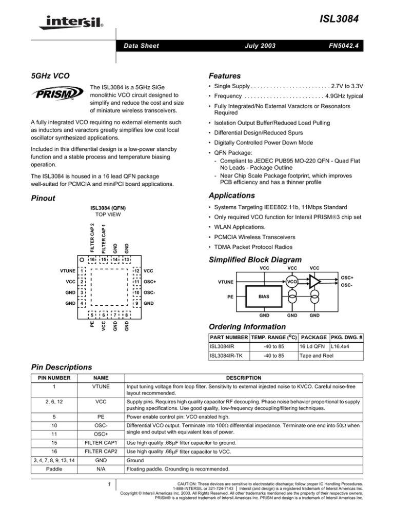
The ISL3084 is housed in a 16 lead QFN package
well-suited for PCMCIA and miniPCI board applications.
• QFN Package:
- Compliant to JEDEC PUB95 MO-220 QFN - Quad Flat
No Leads - Package Outline
- Near Chip Scale Package footprint, which improves
PCB efficiency and has a thinner profile
• TDMA Packet Protocol Radios
16
15
14
13
Simplified Block Diagram
• Only required VCO function for Intersil PRISM3 chip set
• PCMCIA Wireless Transceivers
VTUNE
1
12 VCC
VCC
2
11 OSC+
GND
3
10 OSC-
GND
4
9
VCC
5
6
7
8
PE
VCC
GND
GND
VCC
OSC+
VCO
VTUNE
PE
VCC
OSC-
BIAS
GND
GND
GND
GND
Ordering Information
PART NUMBER TEMP. RANGE (oC) PACKAGE PKG. DWG. #
ISL3084IR
-40 to 85
16 Ld QFN
ISL3084IR-TK
-40 to 85
Tape and Reel
L16.4x4
Pin Descriptions
PIN NUMBER
NAME
1
VTUNE
2, 6, 12
VCC
5
PE
DESCRIPTION
Input tuning voltage from loop filter. Sensitivity to external injected noise to KVCO. Careful noise-free
layout recommended.
Supply pins. Requires high quality capacitor RF decoupling. Phase noise behavior proportional to supply
pushing specifications. Use good quality, low-frequency decoupling/filtering techniques.
Power enable control pin: VCO enabled high.
10
OSC-
11
OSC+
15
FILTER CAP1
Differential VCO output. Terminate into 100Ω differential impedance. Terminate one end into 50Ω when
single end output with equivalent loss of power.
Use high quality .68µF filter capacitor to ground.
Use high quality .68µF filter capacitor to VCC.
16
FILTER CAP2
3, 4, 7, 8, 9, 13, 14
GND
Ground
Paddle
N/A
Floating paddle. Grounding is recommended.
1
CAUTION: These devices are sensitive to electrostatic discharge; follow proper IC Handling Procedures.
1-888-INTERSIL or 321-724-7143 | Intersil (and design) is a registered trademark of Intersil Americas Inc.
Copyright © Intersil Americas Inc. 2003. All Rights Reserved. All other trademarks mentioned are the property of their respective owners.
PRISM® is a registered trademark of Intersil Americas Inc. PRISM and design is a trademark of Intersil Americas Inc.
ISL3084
Absolute Maximum Ratings
Thermal Information
Supply Voltage. . . . . . . . . . . . . . . . . . . . . . . . . . . . . . . . . . . . . . 3.6V
Voltage on Any Other Pin . . . . . . . . . . . . . . . . . . -0.3 to VCC +0.3V
VCC to VCC Decouple . . . . . . . . . . . . . . . . . . . . . . . . . -0.3 to +0.3V
Any GND to GND. . . . . . . . . . . . . . . . . . . . . . . . . . . . . -0.3 to +0.3V
Thermal Resistance (Typical, Note 1)
θJA (oC/W)
θJC (oC/W)
QFN Package. . . . . . . . . . . . . . . . . . . .
47
9
Junction Temperature (Plastic Package) . . . . . . . . . . . . . . . .150oC
Maximum Storage Temperature Range . . . . . . . . . -65oC to 150oC
For recommended soldering conditions see Tech Brief TB389.
Operating Conditions
Temperature Range. . . . . . . . . . . . . . . . . . . . . . . . . . . .-40o to 85oC
Supply Voltage Range . . . . . . . . . . . . . . . . . . . . . . . . . . 2.7V to 3.3V
CAUTION: Stresses above those listed in “Absolute Maximum Ratings” may cause permanent damage to the device. This is a stress only rating and operation of the
device at these or any other conditions above those indicated in the operational sections of this specification is not implied.
NOTE:
1. θJA is measured in free air with the component mounted on a high effective thermal conductivity test board with “direct attach” features. θJC, the
“case temp” is measured at the center of the exposed metal pad on the package underside. See Tech Brief TB379.
General DC Electrical Specifications
TA = 25oC
PARAMETER
MIN
TYP
MAX
UNITS
2.7
-
3.0
V
Supply Current @ 3.3V
-
-
20
mA
Power Down Supply Current
-
-
100
µA
Power Up Time, Filtering dependent
-
50
-
µs
Power Down Time
-
-
1
µs
CMOS Low-Level Input Voltage
-
-
0.3*VCC
V
CMOS High-Level Input Voltage
0.7*VCC
-
-
V
-10
-
10
µA
Supply Voltage
CMOS High- or Low-Level Input Current
AC Electrical Specifications
VCC = 2.7 to 3.3V, Vtune operation from 0.5 to 2.2V, TA = 25oC
PARAMETER
TEST CONDITIONS
RF Frequency Ranges
MIN
TYP
MAX
UNITS
Vtune = 0.5V
-
4.67
4.79
GHz
Vtune = 1.35V
-
4.92
-
GHz
Vtune = 2.2V
5.0
5.19
-
GHz
Tuning Voltage Temperature Coefficient
Vtune = 1.35V, -40 to 85oC
-
40
-
MHz
Tuning Pin Input Leakage
Vtune = 2.0V
-
-
2
µA
VCO Gain
Vtune = 1.35V
250
300
350
MHz/V
VCO Gain Temperature Coefficient
Vtune = 1.35V, -40 to 85oC
-
20
-
MHz/V
Phase Noise
Offset 10kHz
65
70
-
dBc/Hz
Offset 100kHz
-
95
-
dBc/Hz
Phase Noise Temperature Coefficient
Offset @ 10kHz, 0 to 85oC
-
1
4
dB
Integrated Phase Noise @ 5GHz.
10kHz to 1MHz
-
1.6
-
deg_rms
Output Power
Differential into 100Ω
-9
-4
-
dBm
Supply Pushing
VCC = 2.7V–3.3V, across Vtune range
-3
+2
+10
MHz
Load Pulling
VSWR = 2:1
-
1.8
-
MHz
Output VSWR
2:1 BALUM
-
1.3:1
-
-
2
ISL3084
Typical Application
1000P
WELL FILTERED VCC
3.9pF
0.68
GND
GND
VCC
VTUNE
OSC-
GND
GND
GND
GND
GND
OSC+
VCC
VCC
PE
PLL
LOOP FILTER
FILTER
CAP2
FILTER
CAP1
0.68
POWER ENABLE
3
3.3pF
LO_OUT
2:1
BALUM
3.3pF
ISL3084
Quad Flat No-Lead Plastic Package (QFN)
Micro Lead Frame Plastic Package (MLFP)
L16.4x4
16 LEAD QUAD FLAT NO-LEAD PLASTIC PACKAGE
(COMPLIANT TO JEDEC MO-220-VGGC ISSUE C)
MILLIMETERS
SYMBOL
MIN
NOMINAL
MAX
NOTES
A
0.80
0.90
1.00
-
A1
-
-
0.05
-
A2
-
-
1.00
A3
b
0.23
D
0.28
9
0.38
5, 8
4.00 BSC
D1
D2
9
0.20 REF
-
3.75 BSC
1.95
2.10
9
2.25
7, 8
E
4.00 BSC
-
E1
3.75 BSC
9
E2
1.95
e
2.10
2.25
7, 8
0.65 BSC
-
k
0.25
-
-
-
L
0.35
0.60
0.75
8
L1
-
-
0.15
10
N
16
2
Nd
4
3
Ne
4
3
P
-
-
0.60
9
θ
-
-
12
9
Rev. 4 10/02
NOTES:
1. Dimensioning and tolerancing conform to ASME Y14.5-1994.
2. N is the number of terminals.
3. Nd and Ne refer to the number of terminals on each D and E.
4. All dimensions are in millimeters. Angles are in degrees.
5. Dimension b applies to the metallized terminal and is measured
between 0.15mm and 0.30mm from the terminal tip.
6. The configuration of the pin #1 identifier is optional, but must be
located within the zone indicated. The pin #1 identifier may be
either a mold or mark feature.
7. Dimensions D2 and E2 are for the exposed pads which provide
improved electrical and thermal performance.
8. Nominal dimensions are provided to assist with PCB Land Pattern
Design efforts, see Intersil Technical Brief TB389.
9. Features and dimensions A2, A3, D1, E1, P & θ are present when
Anvil singulation method is used and not present for saw
singulation.
10. Depending on the method of lead termination at the edge of the
package, a maximum 0.15mm pull back (L1) maybe present. L
minus L1 to be equal to or greater than 0.3mm.
All Intersil U.S. products are manufactured, assembled and tested utilizing ISO9000 quality systems.
Intersil Corporation’s quality certifications can be viewed at www.intersil.com/design/quality
Intersil products are sold by description only. Intersil Corporation reserves the right to make changes in circuit design, software and/or specifications at any time without
notice. Accordingly, the reader is cautioned to verify that data sheets are current before placing orders. Information furnished by Intersil is believed to be accurate and
reliable. However, no responsibility is assumed by Intersil or its subsidiaries for its use; nor for any infringements of patents or other rights of third parties which may result
from its use. No license is granted by implication or otherwise under any patent or patent rights of Intersil or its subsidiaries.
For information regarding Intersil Corporation and its products, see www.intersil.com
4


![Iin Vin Vin and Iin are the values given in [Series Impedance] Vload](http://s2.studylib.net/store/data/018206929_1-d327defc9b9e133751f2a98335f9c6fb-300x300.png)