Special ESD Considerations for the HS-65643RH
and HS-65647RH Radiation Hardened SOS SRAMs
TM
Application Note
June 1992
The HS-65643RH and HS-65647RH SRAMs are fabricated
on TSOS4, an advanced 1.25mm dual level metal silicon on
sapphire process. The sapphire substrate used in this process is an excellent electrical insulator, and allows the
SRAMs to operate in a wide variety of extremely severe radiation environments; however, the sapphire is also a good
thermal insulator, which makes dissipation of heat generated
in ESD protection devices difficult. This situation leads to
ESD immunity levels of 1000V - 2000V (HBM testing) for
these SRAMs.
Until recently, the human body model (HBM) was the
accepted standard for the evaluation of a semiconductor’s
susceptibility to electrostatic discharge induced damage.
The charged device model (CDM) was proposed by Speakman (1) in 1974 to more accurately model the electrostatic
discharges most commonly resulting in damage to current
generation, small geometry semiconductors; the CDM is
now generally accepted as the best approximation to
charged metal surfaces, the worst case situation generally
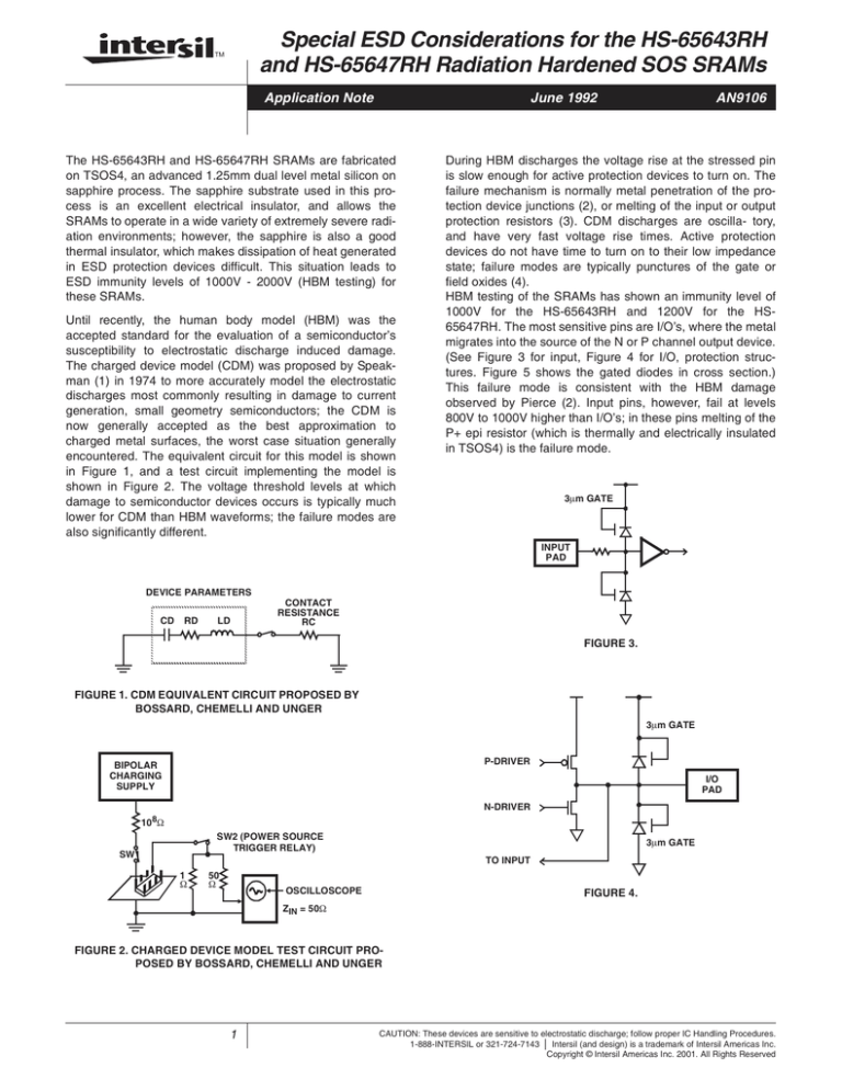
encountered. The equivalent circuit for this model is shown
in Figure 1, and a test circuit implementing the model is
shown in Figure 2. The voltage threshold levels at which
damage to semiconductor devices occurs is typically much
lower for CDM than HBM waveforms; the failure modes are
also significantly different.
AN9106
During HBM discharges the voltage rise at the stressed pin
is slow enough for active protection devices to turn on. The
failure mechanism is normally metal penetration of the protection device junctions (2), or melting of the input or output
protection resistors (3). CDM discharges are oscilla- tory,
and have very fast voltage rise times. Active protection
devices do not have time to turn on to their low impedance
state; failure modes are typically punctures of the gate or
field oxides (4).
HBM testing of the SRAMs has shown an immunity level of
1000V for the HS-65643RH and 1200V for the HS65647RH. The most sensitive pins are I/O’s, where the metal
migrates into the source of the N or P channel output device.
(See Figure 3 for input, Figure 4 for I/O, protection structures. Figure 5 shows the gated diodes in cross section.)
This failure mode is consistent with the HBM damage
observed by Pierce (2). Input pins, however, fail at levels
800V to 1000V higher than I/O’s; in these pins melting of the
P+ epi resistor (which is thermally and electrically insulated
in TSOS4) is the failure mode.
3µm GATE
INPUT
PAD
DEVICE PARAMETERS
CD
RD
LD
CONTACT
RESISTANCE
RC
FIGURE 3.
FIGURE 1. CDM EQUIVALENT CIRCUIT PROPOSED BY
BOSSARD, CHEMELLI AND UNGER
3µm GATE
P-DRIVER
BIPOLAR
CHARGING
SUPPLY
I/O
PAD
N-DRIVER
10 8Ω
SW2 (POWER SOURCE
TRIGGER RELAY)
SW1
3µm GATE
TO INPUT
1
Ω
50
Ω
OSCILLOSCOPE
FIGURE 4.
ZIN = 50Ω
FIGURE 2. CHARGED DEVICE MODEL TEST CIRCUIT PROPOSED BY BOSSARD, CHEMELLI AND UNGER
1
CAUTION: These devices are sensitive to electrostatic discharge; follow proper IC Handling Procedures.
1-888-INTERSIL or 321-724-7143 | Intersil (and design) is a trademark of Intersil Americas Inc.
Copyright © Intersil Americas Inc. 2001. All Rights Reserved
Application Note 9106
References
INPUT
P+ EPI
GND
VDD
N+
N-
N+
P+
3µm
N-
P+
3µm
FIGURE 5. TSOS4 GATED DIODE INPUT
CDM testing of the HS-65643RH and 65647RH has not yet
been performed. Failure modes for HBM testing of TSOS4
material are consistent with those already documented for JI
material; results of CDM waveform testing for the TSOS4
devices are also expected to yield correspondingly lower
immunity levels.
[1] T. S. Speakman, ‘‘A Model for Failure of Bipolar Silicon
Integrated Circuits Subject to Electrostatic Discharge.’’
12th Annual Proceedings of the Reliability Physics
Symposium, pp. 60-69, April 1974.
[2] D. G. Pierce, ‘‘Electro-Thermomigration as an Electrical
Overstress Failure Mechanism.’’ EOS/ESD Symposium
Proceedings, pp. 67-76, 1986.
[3] J. E. Clark, ‘‘TSOS4 ESD Test Results and Failure Analysis,’’ internal Intersil Semi. memo, 20 August, 1990.
[4] L. R. Avery, ‘‘Charged Device Model Testing; Trying to
Duplicate Reality,’’ EOS/ESD Symposium Proceedings,
pp 88-92, 1987.
The fairly low ESD immunity levels characteristic of these
SRAMs (and consequently, of other circuits produced on
SOS processes) dictate that ESD prevention measures be
scrupulously administered. Precautions related to grounding
personnel and work stations are insufficient; any automated
handling equipment must be carefully evaluated for accumulation of CDM-like static charge. A good static control program will allow the use of these high performance, extremely
hard devices while maintaining the highest quality and reliability standards designed and built into them.
All Intersil products are manufactured, assembled and tested utilizing ISO9000 quality systems.
Intersil Corporation’s quality certifications can be viewed at www.intersil.com/design/quality
Intersil products are sold by description only. Intersil Corporation reserves the right to make changes in circuit design, software and/or specifications at any time without
notice. Accordingly, the reader is cautioned to verify that data sheets are current before placing orders. Information furnished by Intersil is believed to be accurate and
reliable. However, no responsibility is assumed by Intersil or its subsidiaries for its use; nor for any infringements of patents or other rights of third parties which may result
from its use. No license is granted by implication or otherwise under any patent or patent rights of Intersil or its subsidiaries.
For information regarding Intersil Corporation and its products, see www.intersil.com
Sales Office Headquarters
NORTH AMERICA
Intersil Corporation
7585 Irvine Center Drive
Suite 100
Irvine, CA 92618
TEL: (949) 341-7000
FAX: (949) 341-7123
Intersil Corporation
2401 Palm Bay Rd.
Palm Bay, FL 32905
TEL: (321) 724-7000
FAX: (321) 724-7946
2
EUROPE
Intersil Europe Sarl
Ave. C - F Ramuz 43
CH-1009 Pully
Switzerland
TEL: +41 21 7293637
FAX: +41 21 7293684
ASIA
Intersil Corporation
Unit 1804 18/F Guangdong Water Building
83 Austin Road
TST, Kowloon Hong Kong
TEL: +852 2723 6339
FAX: +852 2730 1433
