Packaging Commercial CMOS Chips for Lab on a
advertisement

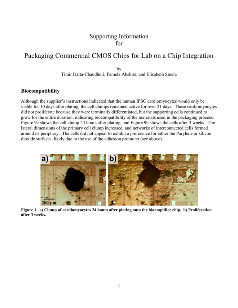
Supporting Information for Packaging Commercial CMOS Chips for Lab on a Chip Integration by Timir Datta-Chaudhuri, Pamela Abshire, and Elisabeth Smela Biocompatibility Although the supplier’s instructions indicated that the human IPSC cardiomyocytes would only be viable for 10 days after plating, the cell clumps remained active for over 21 days. These cardiomyocytes did not proliferate because they were terminally differentiated, but the supporting cells continued to grow for the entire duration, indicating biocompatibility of the materials used in the packaging process. Figure 9a shows the cell clump 24 hours after plating, and Figure 9b shows the cells after 3 weeks. The lateral dimensions of the primary cell clump increased, and networks of interconnected cells formed around its periphery. The cells did not appear to exhibit a preference for either the Parylene or silicon dioxide surfaces, likely due to the use of the adhesion promoter (see above). Figure 1. a) Clump of cardiomyocytes 24 hours after plating onto the bioamplifier chip. b) Proliferation after 3 weeks. 1 Fabrication Figure 2. Profilometry scan (Dektak III) of an edge of a “dummy” 3 x 3 mm silicon die within an epoxy handle wafer. There is a trench at the edge of the die located at 550 µm on the x-axis. The depth of the trench is 500 nm with respect to the edge of the die and 900 nm with respect to the epoxy handle wafer over a lateral distance of 25 µm. Around the chip there is a fall-off of 4 µm over a distance of 350 µm, corresponding to a slope 0.65°. Figure 3. The surface of a chip embedded in epoxy after metal (Cr/Au) deposition. a) At lower magnification the metal may appear to be discontinuous, but b) further magnification reveals that the metal is indeed continuous across the chip edge and onto the epoxy substrate. 2 Figure 4. The chip after it is masked with photoresist to permit selective deposition of PEDOT:PSS onto the recording and reference electrodes. (The green color of the image results from the filter used in the microscope to protect the resist from exposure.) Figure 5. The electrodeposition setup for PEDOT:PSS, which occurs after the handle wafer containing the chip is covered with Au. The Au, masked with photo resist (Figure 12), serves as the working electrode for the constant-current electrodeposition and is contacted by the alligator clip on the left hand side. The counter electrode is the carbon bar shown hanging vertically above the chip. The aqueous monomercontaining electrolyte can be seen between the working and counter electrodes. 3 Figure 6. Close-up of the chip surface after selective PEDOT:PSS deposition. Figure 7. The edge of a chip after the photolithography step for the metal etching step. Thick resist has been patterned to protect the metal traces that connect to the bond pads. After developing the resist was reflowed to increase adhesion to the underlying materials. 4 Figure 8. The corner of a packaged chip after metal etching. Au traces contact the bond pads of the chip. The dark area around the chip is the epoxy handle wafer. Figure 9. The edge of a chip after deposition of the Parylene passivation layer over the entire wafer, but before the Parylene has been etched. The active area of the chip was protected before Parylene deposition using a thick layer of resist, which allows the subsequent etch procedure to leave behind a clean surface that was never in contact with Parylene. The metal etch on this particular chip was performed using a revised version of the mask that allowed for greater overlap of the metal traces over the bond pads. 5 Figure 10. The PCB that provides connections between the packaged chip and a data acquisition system. The PCB has two layers that are connected by a ribbon cable. The bottom layer provides a power supply and bias voltages, as well as connection headers for two data acquisition cables. The top layer of the PCB has spring-loaded Au contact pins that contact the exposed pads at the edges of the wafer. Figure 11. An image of a capacitance sensor IC packaged using the method described in this work. The electrodes were not exposed to the fluid medium. The cells cultured on its surface are kidney cells from Cercopithecus aethiops. No biological adhesion promoter was used. It can be seen from the complete absence of cells on the Parylene that the cells preferred the chip surface. 6 Figure 12. Rat cortical neurons (Invitrogen Cat. No. A10840-01) cultured on the surface of a packaged bioamplfier IC. This image was taken on the 9th day in vitro (DIV 9). The cells were plated onto the chip after a cell adhesion promoter (poly-D-lysine, SIGMA P6407) was applied following the suppliers instructions. Arrows labeled “neurons” indicate some of the cell bodies, and arrows labeled “axons” indicate projecting processes that are forming an interconnected neural network. Two differential recording electrodes from an amplifier are also shown. The large black square in the center is a reference electrode. The electrodes are coated in PEDOT:PSS. Figure 13. The effect of Pt and PEDOT:PSS coatings over Au electrodes on the impedance between an electrode and an electrolyte solution (phosphate buffered saline). Electrochemical impedance spectroscopy was performed using a potentiostat/galvanostat (Eco Chemie, Autolab) with a module for frequency response analysis (FRA). The vertical line marks 1 kHz (the frequency of interest for neural recordings) at which the impedance is decreased by nearly two orders of magnitude when the electrodes are coated with PEDOT:PSS compared to bare Au. 7 Table Metrics The metrics in Table 1 were evaluated from the data presented in the publications. Numerical values are listed when they were given in the source material, but in many cases this was impossible, and metrics had to be estimated. • Chip size was reported in almost all cases. In the one case in which it was estimated, we used a known feature size in the image as a reference. • Area efficiency was estimated as either low (L) or high (H) except when it was possible to calculate it based on data provided in the source. • Estimates of lifetime were based on the passivation material and method. • Barrier distance was estimated from images of the chip using known chip dimensions. • In counting the number of processing steps, deposition and patterning of a material were considered to be one step. (Photoresist baking, for example, was included in this step.) • When vertical step height was not reported, it was estimated to be either large (meaning prohibitive to processing) or low (one could spin resist on it). In some cases the step height was reported in the table as bond wire or chip height, BW/C, indicating that the chip was in a carrier and wire bonded. • Whether post-processing was possible was determined by the surface topography after the chip was packaged. In some cases it was possible to post-process the chip before the package was completed, and this was reported as possible before packaging, BP. 8


