Photo-Thermoelectric Effect at a Graphene Interface
advertisement
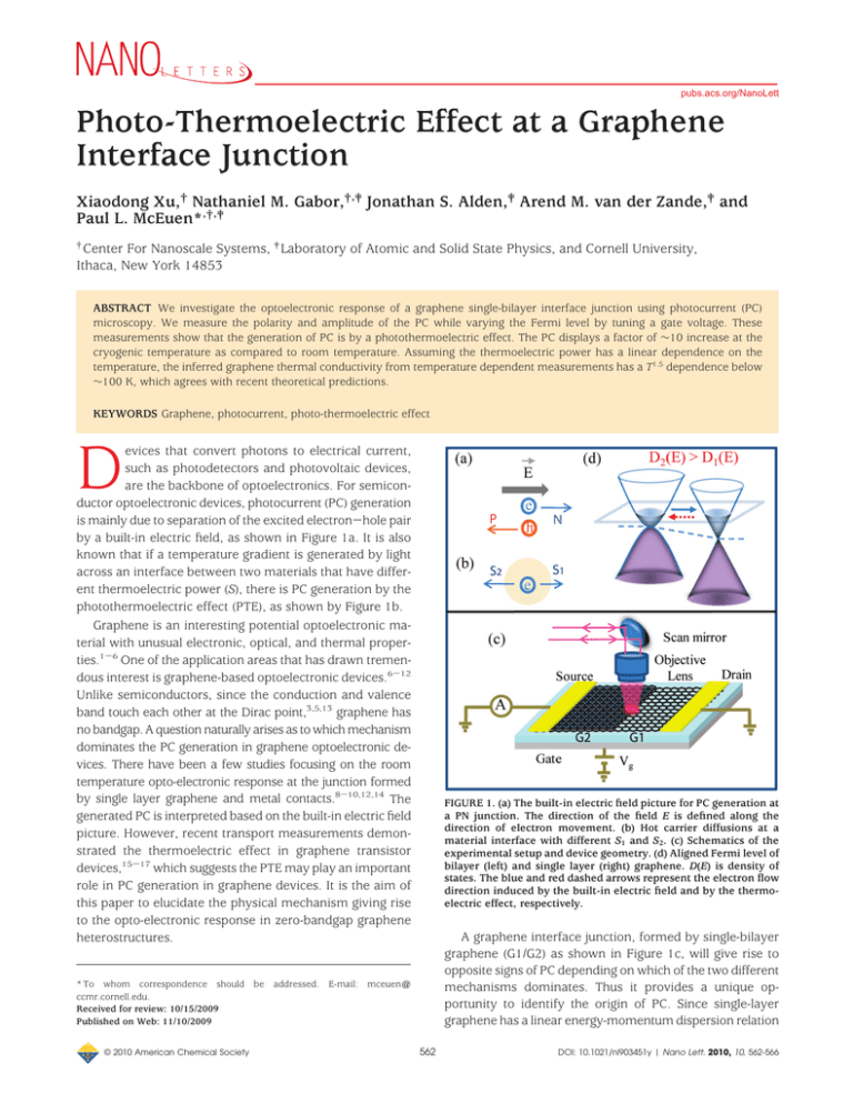
pubs.acs.org/NanoLett Photo-Thermoelectric Effect at a Graphene Interface Junction Xiaodong Xu,† Nathaniel M. Gabor,†,‡ Jonathan S. Alden,‡ Arend M. van der Zande,‡ and Paul L. McEuen*,†,‡ † Center For Nanoscale Systems, ‡ Laboratory of Atomic and Solid State Physics, and Cornell University, Ithaca, New York 14853 ABSTRACT We investigate the optoelectronic response of a graphene single-bilayer interface junction using photocurrent (PC) microscopy. We measure the polarity and amplitude of the PC while varying the Fermi level by tuning a gate voltage. These measurements show that the generation of PC is by a photothermoelectric effect. The PC displays a factor of ∼10 increase at the cryogenic temperature as compared to room temperature. Assuming the thermoelectric power has a linear dependence on the temperature, the inferred graphene thermal conductivity from temperature dependent measurements has a T1.5 dependence below ∼100 K, which agrees with recent theoretical predictions. KEYWORDS Graphene, photocurrent, photo-thermoelectric effect D evices that convert photons to electrical current, such as photodetectors and photovoltaic devices, are the backbone of optoelectronics. For semiconductor optoelectronic devices, photocurrent (PC) generation is mainly due to separation of the excited electron-hole pair by a built-in electric field, as shown in Figure 1a. It is also known that if a temperature gradient is generated by light across an interface between two materials that have different thermoelectric power (S), there is PC generation by the photothermoelectric effect (PTE), as shown by Figure 1b. Graphene is an interesting potential optoelectronic material with unusual electronic, optical, and thermal properties.1-6 One of the application areas that has drawn tremendous interest is graphene-based optoelectronic devices.6-12 Unlike semiconductors, since the conduction and valence band touch each other at the Dirac point,3,5,13 graphene has no bandgap. A question naturally arises as to which mechanism dominates the PC generation in graphene optoelectronic devices. There have been a few studies focusing on the room temperature opto-electronic response at the junction formed by single layer graphene and metal contacts.8-10,12,14 The generated PC is interpreted based on the built-in electric field picture. However, recent transport measurements demonstrated the thermoelectric effect in graphene transistor devices,15-17 which suggests the PTE may play an important role in PC generation in graphene devices. It is the aim of this paper to elucidate the physical mechanism giving rise to the opto-electronic response in zero-bandgap graphene heterostructures. FIGURE 1. (a) The built-in electric field picture for PC generation at a PN junction. The direction of the field E is defined along the direction of electron movement. (b) Hot carrier diffusions at a material interface with different S1 and S2. (c) Schematics of the experimental setup and device geometry. (d) Aligned Fermi level of bilayer (left) and single layer (right) graphene. D(E) is density of states. The blue and red dashed arrows represent the electron flow direction induced by the built-in electric field and by the thermoelectric effect, respectively. A graphene interface junction, formed by single-bilayer graphene (G1/G2) as shown in Figure 1c, will give rise to opposite signs of PC depending on which of the two different mechanisms dominates. Thus it provides a unique opportunity to identify the origin of PC. Since single-layer graphene has a linear energy-momentum dispersion relation * To whom correspondence should be addressed. E-mail: mceuen@ ccmr.cornell.edu. Received for review: 10/15/2009 Published on Web: 11/10/2009 © 2010 American Chemical Society 562 DOI: 10.1021/nl903451y | Nano Lett. 2010, 10, 562-566 and bilayer has a quadratic dispersion relation, the density of states of single-layer (D1(E) ∝ E) is smaller than that of bilayer (D2(E) ∝ finite constant) when the Fermi energy (Ef) is not far away from the Dirac point. Thus, for the same charge density, |Ef| of a single-layer is larger than that of the bilayer, that is, there is a built-in potential difference. The alignment of the Fermi level between single and bilayer graphene leads to the Dirac point of the single layer being lower than the bilayer, as shown in Figure 1d. According to the electric field picture, the photoexcited electrons would be expected to flow from the bilayer to the singlelayer, shown by the blue arrow, and result in a positive PC in the present experimental setup. However, if the PTE is the mechanism generating PC, the magnitude of the generated PC is directly proportional to the difference in S, which is also a measure of the partial molar entropy. Since entropy is proportional to the density of states (D(E)), from the second law of thermodynamics, the hot carriers tend to diffuse to the material with larger D(E) to maximize the entropy. Since D2(E) > D1(E), the electrons should flow from the single to the bilayer and result in a negative PC, shown by the red dashed arrow. By identifying the sign of the PC experimentally, we can determine which mechanism dominates. The graphene device is fabricated by mechanical exfoliation of graphite sheets onto a 90 nm SiO2/Si wafer.4 The single and bilayer graphene are identified by optical contrast and Raman spectroscopy.18 Au/Cr or Au/Ti electrodes are deposited using photolithographic patterning or shadow mask techniques. The device is held in a vacuum cryostat with a temperature control from ∼10 to 300 K. The PC and the correlated reflection image are simultaneously obtained by scanning the laser across the device.8-10,12 The laser excitation wavelength is fixed at 635 nm and the laser spot is about 1 µm. All the PC images presented in this work are taken at zero source-drain bias. We have measured eight different devices and obtained consistent results. Figure 2a displays the PC images of device 1 with the same color scale at various gate voltages (Vg) and a temperature of 12 K. Pronounced PC is seen at the graphene-metal contact interface (G/M) and G1/G2. The PC image in Figure 2b is taken by scanning the laser along the dashed white line indicated in the refection image while sweeping the gate voltage continuously. The PC generation at the G/M has been intensively studied and was mainly attributed to carrier separation by the built-in electric field.8-10,12 In the following, we will focus on the optoelectronic response from G1/G2. By tuning the gate voltage Vg from smaller than Vd to larger than Vd, where Vd corresponds to the Dirac point as shown in Figure 2d, the majority carrier in the graphene changes from hole to electron. The PC at G1/G2 switches signs, changing from positive (red) to negative (blue). Figure 2c shows the gate voltage dependence of the PC at G1/G2, which is the linecut across the dashed black line in Figure 2b. The PC amplitude evolves as the gate voltage varies. On © 2010 American Chemical Society FIGURE 2. Data are taken at T ) 12 K. (a) PC images at various gate voltage Vg. (b) The PC image obtained by the laser linescan as a function of Vg. The laser scan position is indicated by the dashed white line in the reflection image. (c) PC response at the center of graphene interface junction (G1/G2) as a function of Vg. The top right (bottom left) inset is the aligned Fermi level between the single and bilayer at the n (p) doping. (d) Conductance measurement of single (blue) and bilayer (black) graphene as a function of Vg. (e) Calculated thermoelectric power difference at G1/G2 as a function of Vg. the hole doping side, the PC amplitude increases first, reaches a maximum, and then decreases as the gate voltage increases. The same observation holds for electron doping. From the above experimental observations, we determine that the PTE dominates the PC generation at G1/G2, rather than the built-in electric field. Our conclusion is primarily based on the fact that dominance by the built-in electric field would result in positive (negative) PC for the electron (hole) doping, which is clearly opposite to the experimental observations. The physical picture for PC generation due to the PTE is the following: after the electrons are excited from the valence band to the conduction band, they initially relax back to the Fermi level on the time scale of approximately femtoseconds by phonon emission and form a hot Fermion distribution.7,11 Since D2(E) is larger than D1(E), the hot free 563 DOI: 10.1021/nl903451y | Nano Lett. 2010, 10, 562-566 carriers tend to diffuse from the single-layer into the bilayer due to the temperature gradient across G1/G2, which leads to a negative (positive) current for electron (hole) doped graphene. To make a quantitative comparison between the theory and experiment, the PC generated by the PTE can be formulated as (S2 - S1)∆T R I) (1) where S is thermoelectric power, R is the resistance, and ∆T is the temperature difference. From the Mott relation,15,16,19 we have the Seebeck coefficient as S)- π2kb2T 1 dG 3e G dE E)Ef FIGURE 3. (a) The bilayer (black line) Dirac point is about 5 V smaller than that of the single-layer (blue line). (b) The generated PC at the G1/G2 as a function of Vg. (c) The calculated S and (d) S2 - S1. (2) where kb is the Boltzmann constant, e is electron charge, T is temperature, G is conductance, and Ef is the Fermi energy. The conductance G is proportional to neµ for graphene, where n is charge density and µ is the electron mobility. When Ef is away from the Dirac point, µ is approximately a constant and S is proportional to D(E). The calculated S2 - S1 as a function of Vg is shown in Figure 2e. In the calculation, the (1/G)[(dG)/(dE)] term is replaced by 1 dG dVg G dVg dE where (dG)/(dVg) can be derived from the conductance measurements. The dependence of Ef on the charge density n can be derived from tight binding calculations.20 For single layer graphene, Ef ) pvF(πn)1/2 and vF is the Fermi velocity. For bilayer FIGURE 4. (a) The amplitude of PC generated at G1/G2 as a function of T. (b) Logarithmic plot of the data in (a). The data are fitted with a line with a slope of -0.5 (-1.5) for below (above) ∼100 K. (c) The PC images at a temperature of 14 K (left) and 295 K (right). at a certain Vg between the two Dirac points, which corresponds to a maximum in the PC data. The calculated S2 S1 for device 2, shown in Figure 3d, qualitatively reproduces the line shape and sign of the PC. We also performed temperature and power dependent studies of PC. We plot the absolute PC amplitude of device 2 at Vg ) -4 V as a function of temperature in Figure 4a. The PC amplitude decreases nonlinearly as the temperature increases. We replot the data on a logarithmic scale in Figure 4b, which can be separated into two regions around a temperature of 100 K. The data are fitted with a line with a slope of -0.5 (-1.5) for below (above) ∼100 K. For instance, the PC images of device 2 at 14 K and at 295 K are also displayed on the left and right of Figure 4c. The PTE naturally explains the temperature dependent data. Equation 1 shows that the PC is proportional to (S2 S1)/κ, where κ is the thermal conductivity. Since S has an √ 1 (2pvF)2πn + 2γ12 - 2γ1√(2pvF)2πn + γ12 2 and γ1 is the interlayer coupling strength. The calculated S2 - S1 qualitatively reproduce the line shape and sign of the experimental data in Figure 2c.21 S2 - S1 reverses sign at Vg ) Vd ) 3.7 V, which is close to the sign switch of PC at 3.4 V. The PTE can account for the experimental results from devices with nonoverlapping Dirac points between the single and bilayer. An example (device 2) is shown by the gate dependent conductance measurement in Figure 3a, where the bilayer Dirac point is ∼5 V lower than that of the singlelayer. The PC at the G1/G2 as a function of Vg is shown in Figure 3(b). When Vg is between the two Dirac points, that is, the single-layer is p-doped but the bilayer is n-doped, S of the single-layer has the opposite sign of bilayer, as shown in Figure 3c. Thus, the difference in S reaches a maximum Ef ) © 2010 American Chemical Society 564 DOI: 10.1021/nl903451y | Nano Lett. 2010, 10, 562-566 5b. A line fit with a slope of ∼1 corresponds to the data in the linear region. With strong laser power, the PC shows a P0.8 dependence, which is in excellent agreement with the prediction from the PTE picture. A final question is whether the PC at a G/M or the interface P-N junction is also generated by the PTE. We know that S is negative for electrons and positive for holes in graphene. For the G/M, the thermal voltage drives electrons (holes) from the metal contact to the graphene for the n- (p-) doping, which leads to positive (negative) PC at the source and negative (positive) at the drain. The PC reverses polarity as the majority carrier changes from electron to hole. For the P-N junctions formed inside the graphene, the hot electrons also diffuse from the P to the N channel. The above explanations are consistent with the experimental observations at the G/M and PN junctions. Furthermore, we have done other measurements (data not shown) on the PC generation at G/M and PN junctions. The results show similar features as G1/ G2, such as comparable PC amplitude, PC saturation at low temperatures, and similar temperature dependence. Although we cannot rule out the built-in electric field picture, the agreement between the theoretical explanations and the experimental results strongly indicates that PTE may also be the origin of the PC in G/M and P-N junction devices. In summary, we have demonstrated that the PTE gives rise to the PC generation at graphene interface field-effect transistors. This understanding will have potential impact for designing graphene-based optoelectronics, such as photothermocouples and photovoltaics. Since the PTE at the graphene interface arises from the difference in the DOS between single and bilayer, the excellent agreement between the experimental observation and the PTE interpretation demonstrates that the scanning PC microscopy can be a local probe of the DOS. Thus, we can use the scanning PC technique for spatially probing novel physics arising from the graphene interface structure, such as anomalous quantum oscillations with a strong magnetic field,27 edge electronic states,28 and graphene edge chemical functionalization.29 FIGURE 5. Power dependent PC amplitude generated at G1/G2 at a temperature of 30 K. (a) Linear and (b) logarithmic plots. Saturation power is defined as the power corresponding to the PC deviating 10% from the linear region. approximate T1 dependence13,14 and κ has a power law dependence of Tβ with β > 1,22-25 PC is expected to have a nonlinear dependence of 1/Tβ-1, which agrees with the experimental results. Since the slope in Figure 4b corresponds to 1 - β, we infer that κ has a T1.5 (T2.5) dependence below (above) ∼100 K. The T2.5 dependence at high temperature is similar to κ of the graphite.23 The T1.5 dependence at low temperature agrees with the recent theoretical prediction of graphene κ.22-25 It suggests that at low temperature, the out-of-plane acoustic phonon mode, which has a quadratic dispersion relation, contributes to the thermal conductivity. The observation also indicates that the phonon-induced κ dominates the electron-induced κ when Vg is close to Vd.25 We can estimate the magnitude of the PC generated by the PTE using eqs 1 and 2. κ of single-layer graphene has been reported as 5 × 10³ W/m·K at room temperature.4 Taking the heat flow as a radial wave, given that κ2πh∆T ) PR, where h is the thickness of graphene of ∼3 Å, P is incident laser power of 40 µW, and R is the absorption coefficient of 2.3%, we infer that ∆T is on the order of ∼0.1 K. Taking (S2 - S1) on the order of 100 µV/K by calculation from eq 1 and the resistance of graphene on the order of 5 kΩ/µm2, the PC is on the order of ∼2 nA, which is consistent with the experimental observations at room temperature.26 With the knowledge of κ and S as functions of T, we should be able to predict the power dependence of the PC at low temperature. From eqs 1 and 2, we have I ∝ T∆T. When the laser power is strong enough, the induced temperature difference ∆T dominates. Thus, ∆T can be approximately taken as T, which leads to I ∝ T2. On the other hand, from κ∆T ∝ P and κ ∝ Tβ, we have T ∝ P1/(β+1), which leads to I ∝ P2/(β+1). Taking β ) 1.5 from the temperature dependent measurement, we expect that the PC should have P0.8 dependence for strong laser power at low temperature. The obtained laser-power-dependent PC measurements confirm the above predictions. Taking the PC amplitude as a function of laser power at T ) 30 K as an example, shown in Figure 5a, we observe a PC saturation effect. The blue line is a guide to the eye and the PC deviates from the linear dependence around 20 µW (corresponding to ∼0.7 kW/ cm2). The data are replotted on a logarithmic scale in Figure © 2010 American Chemical Society Acknowledgment. This work is supported by the NSF through the Cornell Center for Nanoscale Systems and Center for Materials Research, and by the MARCO Focused Research Center on Materials, Structures, and Devices. Device fabrication is performed at the Cornell Nano-Scale Science and Technology Facility, funded by NSF. REFERENCES AND NOTES (1) (2) (3) (4) 565 Balandin, A. A.; Ghosh, S.; Bao, W.; Calizo, I.; Teweldebrhan, D.; Miao, F.; Lau, C. N. Nano Lett. 2008, 8 (3), 902. Chen, J.-H.; Jang, C.; Xiao, S.; Ishigami, M.; Fuhrer, M. S. Nat. Nanotechnol. 2008, 3 (4), 206. Novoselov, K. S.; Geim, A. K.; Morozov, S. V.; Jiang, D.; Katsnelson, M. I.; Grigorieva, I. V.; Dubonos, S. V.; Firsov, A. A. Nature 2005, 438 (7065), 197. Novoselov, K. S.; Geim, A. K.; Morozov, S. V.; Jiang, D.; Zhang, Y.; Dubonos, S. V.; Grigorieva, I. V.; Firsov, A. A. Science 2004, 306 (5696), 666. DOI: 10.1021/nl903451y | Nano Lett. 2010, 10, 562-566 (5) (6) (7) (8) (9) (10) (11) (12) (13) (14) (15) (16) Zhang, Y.; Tan, Y.-W.; Stormer, H. L.; Kim, P. Nature 2005, 438 (7065), 201. Zhang, Y.; Tang, T.-T.; Girit, C.; Hao, Z.; Martin, M. C.; Zettl, A.; Crommie, M. F.; Shen, Y. R.; Wang, F. Nature 2009, 459 (7248), 820. George, P. A.; Strait, J.; Dawlaty, J.; Shivaraman, S.; Chandrashekhar, M.; Rana, F.; Spencer, M. G. Nano Lett. 2008, 8 (12), 4248. LeeEduardo, J. H.; Balasubramanian, K.; Weitz, R. T.; Burghard, M.; Kern, K. Nat Nano 2008, 3 (8), 486. Mueller, T.; Xia, F.; Freitag, M.; Tsang, J.; Ph, A. Phys. Rev. B 2009, 79 (24), 245430. Park, J.; Ahn, Y. H.; Ruiz-Vargas, C. Nano Lett. 2009, 9 (5), 1742. Sun, D.; Wu, Z.-K.; Divin, C.; Li, X.; Berger, C.; de Heer, W. A.; First, P. N.; Norris, T. B. Phys. Rev. Lett. 2008, 101 (15), 157402. Xia, F.; Mueller, T.; Golizadeh-Mojarad, R.; Freitag, M.; Lin, Y.m.; Tsang, J.; Perebeinos, V.; Avouris, P Nano Lett. 2009, 9 (3), 1039. Semenoff, G. W. Phys. Rev. Lett. 1984, 53 (26), 2449. Giovannetti, G.; Khomyakov, P. A.; Brocks, G.; Karpan, V. M.; van den Brink, J.; Kelly, P. J. Phys. Rev. Lett. 2008, 101 (2), No. 026803. Wei, P.; Bao, W.; Pu, Y.; Lau, C. N.; Shi, J. Phys. Rev. Lett. 2009, 102 (16), 166808. Zuev, Y. M.; Chang, W.; Kim, P. Phys. Rev. Lett. 2009, 102 (9), No. 096807. © 2010 American Chemical Society (17) Checkelsky, J. G.; Ong, N. P. Phys. Rev. B 2009, 80 (8), No. 081413. (18) Ferrari, A. C.; Meyer, J. C.; Scardaci, V.; Casiraghi, C.; Lazzeri, M.; Mauri, F.; Piscanec, S.; Jiang, D.; Novoselov, K. S.; Roth, S.; Geim, A. K. Phys. Rev. Lett. 2006, 97 (18), 187401. (19) Cutler, M.; Mott, N. F. Phys. Rev. 1969, 181 (3), 1336. (20) McCann, E.; Fal’ko, V. I. Phys. Rev. Lett. 2006, 96 (8), No. 086805. (21) A Strict comparison between the theory and data can be done if both spatial and gate dependence of R and ∆T are available. (22) Foster, M. S.; Aleiner, I. L. Phys. Rev. B 2009, 79 (8), No. 085415. (23) Mingo, N.; Broido, D. A. Phys. Rev. Lett. 2005, 95 (9), No. 096105. (24) Peres, N. M. R.; dos Santos, J. M. B. L.; Stauber, T. Phys. Rev. B 2007, 76 (7), No. 073412. (25) Saito, K.; Nakamura, J.; Natori, A. Phys. Rev. B 2007, 76 (11), 115409. (26) There is a small amount of heat dissipating through the SiO2 layer. For simplicity, we estimate the magnitude of PC by neglecting the heat flow through SiO2. Exact calculation of PC requres more rigorous treatment. (27) Puls, C. P.; Staley, N. E.; Liu, Y. Phys. Rev. B 2009, 79 (23), 235415. (28) Nakada, K.; Fujita, M.; Dresselhaus, G.; Dresselhaus, M. S. Phys. Rev. B 1996, 54 (24), 17954. (29) Wang, X.; Li, X.; Zhang, L.; Yoon, Y.; Weber, P. K.; Wang, H.; Guo, J.; Dai, H. Science 2009, 324 (5928), 768. 566 DOI: 10.1021/nl903451y | Nano Lett. 2010, 10, 562-566
