Multiple Feedback Band-Pass
Design Example
by Hank Zumbahlen,
Analog Devices, Inc.
One could also adjust the output for maximum output,
which also occurs at resonance, but this is usually not as
precise, especially at lower values of Q where there is a less
pronounced peak.
MULTIPLE FEEDBACK BAND-PASS DESIGN
EQUATIONS
IN THIS MINI TUTORIAL
− H ω0 s
A multiple feedback band-pass is designed in this mini
tutorial, one in a series of mini tutorials describing discrete
circuits for op amps.
s + αω 0 s + ω 0 2
2
OUT
C4
C3
R1
R2
Figure 2.
VO
=
V IN
R5
C3
10423-001
IN
R2
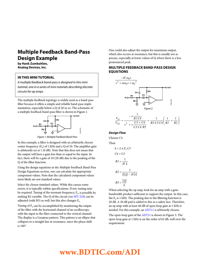
Figure 1. Multiple Feedback Band-Pass
In this example, a filter is designed with an arbitrarily chosen
center frequency (F0) of 1 kHz and a Q of 10. The amplifier gain
is arbitrarily set at 1 (0 dB). Note that this does not mean that
the output will have a gain less than or equal to the input. In
fact, there will be a gain of 10 (20 dB) due to the peaking of the
Q of the filter function.
Using the design equations in the Multiple Feedback Band-Pass
Design Equations section, one can calculate the appropriate
component values. Note that the calculated component values
most likely are not standard values.
Select the closest standard values. While this causes some
errors, it is typically within specifications. If not, tuning may
be required. Tuning of the resonant frequency, F0, is possible by
making R2 variable. The Q of the circuit (see MT-210) can be
adjusted (with R5) as well, but this also changes F0.
Tuning of F0 can be accomplished by monitoring the output
of the filter with the horizontal channel of an oscilloscope,
with the input to the filter connected to the vertical channel.
The display is a Lissajous pattern. This pattern is an ellipse that
collapses to a straight line at resonance, since the phase shift
is 180°.
1
1
R1 C4
1
1
+
+
C3 + C4
R5 C3 C4 R1
R2
+s
C3 C4 R5
−s
OUT
C4
10423-002
IN
The multiple feedback topology is widely used as a band-pass
filter because it offers a simple and reliable band-pass implementation, especially below a Q of 20 or so. The schematic of
a multiple feedback band-pass filter is shown in Figure 1.
R1
R5
s2
Design Flow
Choose C3.
Then
k = 2 π F0 C3
C4 = C3
R1 =
1
Hk
R2 =
1
(2 Q − H ) k
R5 =
2Q
k
When selecting the op amp, look for an amp with a gainbandwidth product sufficient to support the output. In this case,
the F0 is 1 kHz. The peaking due to the filtering function is
20 dB. A 20 dB pad is added to this as a safety fact. Therefore,
an op amp with at least 40 dB of open-loop gain at 1 kHz is
needed. For this example, an AD711 is arbitrarily chosen.
The open-loop gain of the AD711 is shown in Figure 3. The
open-loop gain at 1 kHz is on the order of 65 dB, well over the
requirement.
www.BDTIC.com/ADI
60
60
40
40
20
20
10
0
–20
10
100
1k
10k
100k
1M
–40
–20
10M
–50
10
FREQUENCY (Hz)
100
1k
10k
100k
10k
100k
FREQUENCY (Hz)
Figure 5.
Figure 3. Open-Loop Gain of the AD711
180
If the open-loop gain of the op amp is too low, a phenomenon
known as Q multiplication takes place and the response of the
filter is affected.
The final design for the filter is shown in Figure 4. The standard
values for the resistors have been substituted. Note that this
circuit is shown in National Instrument’s Electronic Workbench.
A version of this program can be downloaded from the Analog
Devices website. In addition, a group of ready-entered circuits,
including this filter, can be download from the same page.
90
PHASE (Degrees)
MULTIPLE FEEDBACK BAND-PASS FILTER FINAL
DESIGN
135
45
0
–45
–90
–135
–180
10
XBP1
100
1k
FREQUENCY (Hz)
IN
–
C1
R1
15.8kΩ 10nF
1%
V3 +
1V p
1kHz –
0°
Figure 6.
OUT
+ –
REFERENCES
C2
10nF
Jung, Walter G., editor. 2006. Op Amp Applications Handbook,
Newnes, ISBN 0-916550-26-5.
R3
316kΩ
1%
2
R2
806Ω
1%
3
Kester, Walt, editor. 1992. Amplifier Applications Guide, Analog
Devices, Inc. ISBN: 0-916550-10-9.
4
U1
6
AD711KN
7
Zumbahlen, Hank, editor. 2007. Basic Linear Design, Analog
Devices, Inc. ISBN 0-916550-28-1.
1 5
V1
12V
V2
12V
Figure 4.
The voltage of this circuit is shown in Figure 5; the phase
response is shown in Figure 6.
10423-004
+
10423-006
RL = 2kΩ
C = 100pF
–20
–30
0
0
–10
10423-005
80
GAIN (dB)
80
20
PHASE MARGIN (Degrees)
100
10423-003
OPEN LOOP GAIN (dB)
100
Zumbahlen, Hank. “Phase Relations in Active Filters.” Analog
Dialogue, Vol. 14, No. 4, 2008.
Zumbahlen, Hank, editor, 2008. Linear Circuit Design
Handbook, Newnes, ISBN 978-0-7506-8703-4.
REVISION HISTORY
2/12—Revision 0: Initial Version
©2012 Analog Devices, Inc. All rights reserved. Trademarks and
registered trademarks are the property of their respective owners.
MT10423-0-2/12(0)
www.BDTIC.com/ADI
