Method to Suppress the Parasitic Resonance Using Parallel
advertisement
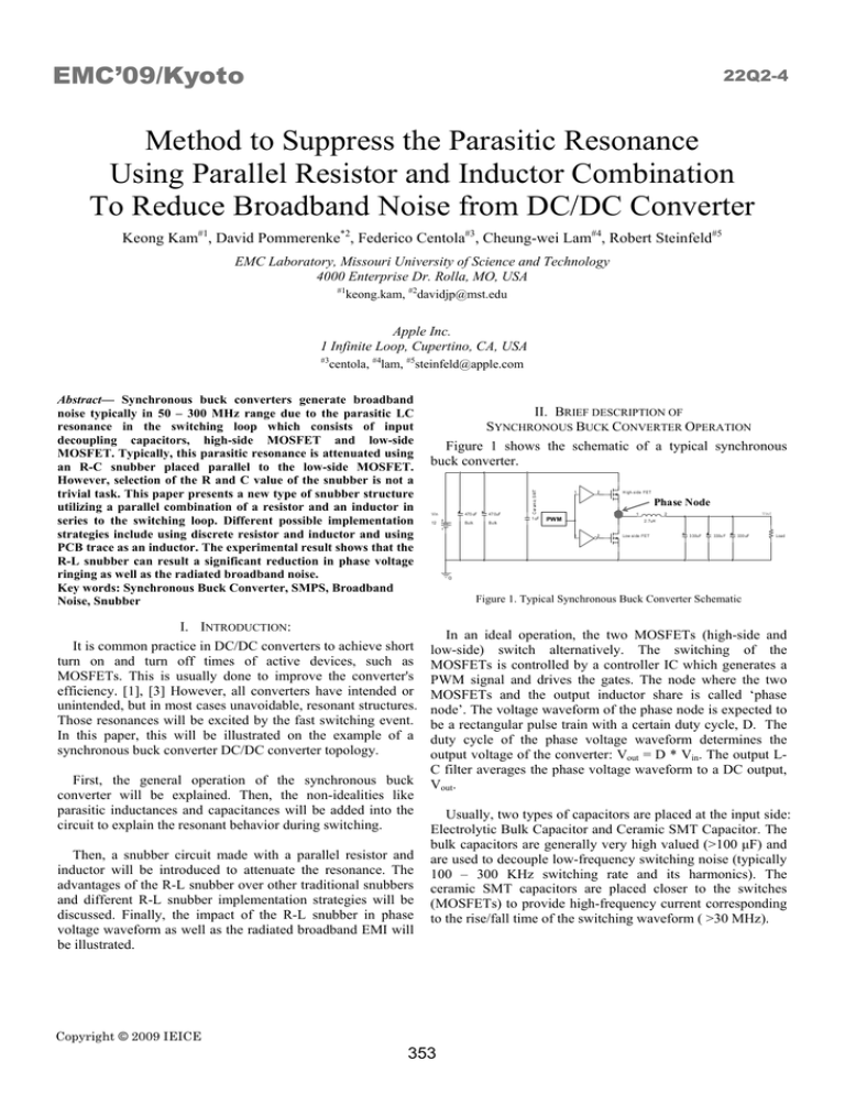
EMC’09/Kyoto 22Q2-4 Method to Suppress the Parasitic Resonance Using Parallel Resistor and Inductor Combination To Reduce Broadband Noise from DC/DC Converter Keong Kam#1, David Pommerenke*2, Federico Centola#3, Cheung-wei Lam#4, Robert Steinfeld#5 EMC Laboratory, Missouri University of Science and Technology 4000 Enterprise Dr. Rolla, MO, USA #1 keong.kam, #2davidjp@mst.edu Apple Inc. 1 Infinite Loop, Cupertino, CA, USA #3 centola, #4lam, #5steinfeld@apple.com I. INTRODUCTION: It is common practice in DC/DC converters to achieve short turn on and turn off times of active devices, such as MOSFETs. This is usually done to improve the converter's efficiency. [1], [3] However, all converters have intended or unintended, but in most cases unavoidable, resonant structures. Those resonances will be excited by the fast switching event. In this paper, this will be illustrated on the example of a synchronous buck converter DC/DC converter topology. First, the general operation of the synchronous buck converter will be explained. Then, the non-idealities like parasitic inductances and capacitances will be added into the circuit to explain the resonant behavior during switching. Then, a snubber circuit made with a parallel resistor and inductor will be introduced to attenuate the resonance. The advantages of the R-L snubber over other traditional snubbers and different R-L snubber implementation strategies will be discussed. Finally, the impact of the R-L snubber in phase voltage waveform as well as the radiated broadband EMI will be illustrated. II. BRIEF DESCRIPTION OF SYNCHRONOUS BUCK CONVERTER OPERATION Figure 1 shows the schematic of a typical synchronous buck converter. Vin 470 uF 47 0uF 12 Bulk Bu lk C eram ic S MT Abstract— Synchronous buck converters generate broadband noise typically in 50 – 300 MHz range due to the parasitic LC resonance in the switching loop which consists of input decoupling capacitors, high-side MOSFET and low-side MOSFET. Typically, this parasitic resonance is attenuated using an R-C snubber placed parallel to the low-side MOSFET. However, selection of the R and C value of the snubber is not a trivial task. This paper presents a new type of snubber structure utilizing a parallel combination of a resistor and an inductor in series to the switching loop. Different possible implementation strategies include using discrete resistor and inductor and using PCB trace as an inductor. The experimental result shows that the R-L snubber can result a significant reduction in phase voltage ringing as well as the radiated broadband noise. Key words: Synchronous Buck Converter, SMPS, Broadband Noise, Snubber 1 uF 1 2 H igh-side F ET Phase Node 1 PWM Vou t 2 2. 7uH 1 2 Low -side F ET 3 30uF 330u F 330 uF Load 0 Figure 1. Typical Synchronous Buck Converter Schematic In an ideal operation, the two MOSFETs (high-side and low-side) switch alternatively. The switching of the MOSFETs is controlled by a controller IC which generates a PWM signal and drives the gates. The node where the two MOSFETs and the output inductor share is called ‘phase node’. The voltage waveform of the phase node is expected to be a rectangular pulse train with a certain duty cycle, D. The duty cycle of the phase voltage waveform determines the output voltage of the converter: Vout = D * Vin. The output LC filter averages the phase voltage waveform to a DC output, Vout. Usually, two types of capacitors are placed at the input side: Electrolytic Bulk Capacitor and Ceramic SMT Capacitor. The bulk capacitors are generally very high valued (>100 ȝF) and are used to decouple low-frequency switching noise (typically 100 – 300 KHz switching rate and its harmonics). The ceramic SMT capacitors are placed closer to the switches (MOSFETs) to provide high-frequency current corresponding to the rise/fall time of the switching waveform ( >30 MHz). Copyright © 2009 IEICE 353 EMC’09/Kyoto 22Q2-4 Trace 1 Trace 2 1 2 2 2 ESL 1 Vin Trace 2 1 1 L_parasitic 2 2 ESL ESL 1 1 2 High-side FET 1 1 PWM 12 470uF 470uF Bulk Bulk Ceramic SMT Buck Converter Testboard Baseline 40 dB PV/m III. ROOT CAUSE OF THE BROADBAND EMI FROM SYNCHRONOUS BUCK CONVERTER Various measurements and simulation results have shown that during the turn on of the high-side FET in a synchronous buck converter circuit, there is a parasitic LC resonance in the switching loop formed by the input decoupling capacitors and the switching FETs. [2] The resonance is due to the switching loop parasitic inductance and the low-side FET output capacitance. Figure 2 shows the input and switching part of the synchronous buck converter with parasitic inductances. The dashed red line in Figure 2 shows the switching loop which forms the LC resonant structure. This resonance causes ringing at the phase voltage, and the ringing frequency observed on the phase voltage coincides with this resonant frequency of the switching loop. 150 200 250 300 Frequency [MHz] 350 400 450 500 For the case of this particular test board, the switching loop resonance occurred at 120 MHz. This broadband noise can prevent an electronic system from passing the regulatory electromagnetic compatibility requirements. In addition, the noise can cause interference within the system like reducing the signal to noise ratio of signals received by an antenna within this system. An example would be an FM radio antenna, receiving at 88-107 MHz and being disturbed by the ringing frequency of the phase voltage of a DC/DC converter. 1 2 IV. EXISTING METHODS FOR REDUCING THE BROADBAND EMI To reduce electromagnetic compatibility problems, the ringing of the phase voltage needs to be attenuated. [3] Traditionally this has been done by one or a combination of the methods listed below: Low-side FET 1) Controlling the rise time. If the rise time is increased, the resonant structures will not be excited as strongly. For the Buck converter this translates to increasing the turn on time of the main FET such that the slower turn on provides less energy at the frequency the resonance in switching loop shown in figure 1. However, this trades off the power efficiency. 2) Adding an R-C snubber circuits parallel to the lowside MOSFET. [4] [5] This method is especially used widely in smaller electronic systems because of its small size and component counts. However, the parasitic inductance associated with the R-C snubber branch can make the snubber difficult to predict without experimental iterations to get the optimum value of the resistor and capacitor. 3) Other circuits including the use clamping diodes, etc can be found in many technical papers. [3], [6] However, some of them require more active components and complex design. Phase Voltage 15 V 10 5 3.9 100 Figure 4.Far-field Radiation from Synchronous Buck Converter Test Board Figure 3 shows a measured phase voltage waveform of the synchronous buck converter test board. This ringing frequency also translates to the broadband radiated noise in the far-field centered around the ringing frequency. 3.88 50 2 1uF 3.86 0 -20 Figure 2. Input and Switching Part of the Synchronous Buck Converter with Parasitic Inductances 3.84 20 2.7uH 0 0 3.82 Vertical Horizontal 3.92 3.94 Ps Figure 3. Ringing in the Phase Voltage Waveform Due to Parasitic Resonance in the Switching Loop Figure 4 shows the measured far-field radiated noise of the same test board. While the methods listed above allow a reduction of the ringing, they have different disadvantages, like their complexity, or the necessity of experimental iterations. Copyright © 2009 IEICE 354 EMC’09/Kyoto 22Q2-4 The first one on the list was implemented on the test board for experimental verification as shown in Figure 5. The second place on the list may be slightly different than the first method depending on the capacitance of the driver. The last one on the list may have additional benefits due to having common source inductance. The benefits include prevention of the shoot-through and accidental c dv/dt turn-on. More detailed information about this can be found on technical papers and literatures. [7], [8] RL Snubber R 0.7 1 L 2 2. 5nH Vin 47 0uF 4 70uF 12 Bu lk B ulk C era mic SM T V. PROPOSED METHOD: R-L SNUBBER Because of the parasitic LC resonance in the switching loop of the synchronous buck converter, there is large ringing current in the switching loop at the resonant frequency. The ringing current can couple to other parts of the circuit to cause EMC problems by many ways. First, by conductive means, thus via the input voltage plane of the converter, or via the output voltage of the converer. Otherwise, it can cause magnetic fields that induce electric fields and consequential voltages or currents in other parts of the electronic system. Furthermore, the ringing in the phase voltage can couple, via small capacitances that are formed between the phase voltage area on the PCB to other parts of the circuit. This coupling is via the displacement current. There are a variety of strategies to reduce the ringing as described in section IV. The purpose of the new proposed method, R-L snubber, is to attenuate the RF noise in the switching loop while passing the low frequency current unattenuated, and as a result, attenuate the phase voltage ringing. 1uF 1 2 H igh-side F ET 1 PWM Vo ut 2 2 .7u H 1 2 L ow-s id e F ET 330u F 330 uF 33 0uF Loa d 0 Figure 5. R-L snubber Implementation By putting a parallel combination of a small resistor and a small inductor, in series to the switching loop, a necessasry RF current attenuation in the switching loop can be achieved. The Q factor of the parasitic LC resonance in the switching loop can be decreased significantly due to the addition of the loss presented by the R-L snubber. Figure 6 shows the comparison of the phase voltage before and after adding the R-L snubber. It shows that the ringing at the phase voltage has been significantly reduced. Phase Voltage Comparison 20 No RL Snubber 18 The inductor can be a discrete inductor, or it can be implemented in PCB. The implementation in PCB is especially effective if the switching loop has been designed to offer a minimal inductance before adding an R-L snubber. For example, if the switching loop is designed in the top layer of a PCB and the second layer is a solid ground plane at a narrow distance, like 0.1 mm, then the inductance of the phase voltage loop can be as low as 3-4 nH. For an R-L snubber to be effective, only a small inductance needs to be added, like 2.5nH. This small inductance can be bridged by a low value resistor of 1 Ohm or less to effecively control the ringing in the phase voltage loop. 14 12 10 8 6 4 2 0 13.08 13.1 13.12 13.14 13.16 13.18 13.2 Figure 6. The Phase Voltage Comparison Before and After R-L Snubber Figure 7 shows the comparison of the measured far-field radiated noise of the test board with and without the R-L snubber. The measured result shows over 12 dB improvement in radiated noise. The R-L snubber can be placed in various places in the switching loop: a) before the high-side FET, b) between high-side source and phase node, c) or between phase node and low-side drain. Copyright © 2009 IEICE 355 Far-field Comparison 30 No RL Snubber 20 dBPV/m For this particular test board, a combination of a 2.5nH discrete inductor and a 0.7ohm resistor was used for the R-L snubber. The reason that the snubber can be effective with such a low value of inductor is because the switching loop size has been minimized in the test board to minimize the parasitic loop inductance. Used along with small switching loop parasitic inductance, the inductance of the R-L snubber can be very small. With 0.733: 2.5nH RL Snubber 16 2.5nH 1: RL Snubber 12dB 10 0 -10 -20 50 100 150 Frequency [MHz] 200 250 Figure 7. Far-field Noise Comparison with R-L snubber 300 EMC’09/Kyoto 22Q2-4 The additional power consumption due to the R-L snubber is small. A PSPICE simulation was performed for the prediction of the power loss due to the R-L snubber. The simulation result shows that for the 18W synchronous buck converter test board used for the experimental verification, the total power loss from the R-L snubber was about 300mW. The power loss through the parallel resistor is very low, such that a 1/5 Watt 0603 SMT resistor is sufficient. The equivalent series resistnace (ESR) of the inductor is the major contributor of the power loss, but the ESR can be reduced to minimum to have neglible effect on efficiency. The ESR of the inductor can be reduced with more efficient inductor design or by implementing the inductor with a PCB trace. VI. CONCLUSION The root cause of the broadband EMI from a synchronous buck converter was discussed. Many experiments and measurements show that the parasitic LC resonance in the switching loop formed by the input decoupling capacitors and the high-side and low-side MOSFETs causes the broadband noise in the synchronous buck converter system. The broadband noise is indicated by the ringing frequency of the phase voltage waveform as well as the far-field noise. the package parasitics and a small resistor as additional external component. . VII. [1] [2] [3] [4] [5] [6] [7] [8] The typical methods for reducing the broadband EMI from this parasitic LC resonance of the synchronous buck converter include controlling the rise/fall time of the switching, R-C snubber, and other clamping snubber using active components. However these methods all have different disadvantages, and the novelty of the proposed methods, R-L snubber circuit is: Simple circuit Predictability Low impact on efficiency Superior suppression of phase voltage ringing A small-sized resistor Possibility of implementing the inductor on the PCB trace The R-L snubber implemented on the synchronous buck converter test board showed significant suppression of phase voltage ringing and up to 12dB decrease in the radiated broadband EMI. The R-L snubber can be best implemented in the switching loop of the synchronous buck converter if the parasitic switching loop inductance is minimized. This can be achieved by placing the decoupling capacitors and the two MOSFETs as close as possible and also by having a solid ground plane under the loop separated by a small dielectric thickness. The possible implementation of the R-L snubber includes not only using discrete components, but also using a PCB trace as an inductor. It may be possible to integrate the R-L snubber inside a MOSFET package using the inductance of Copyright © 2009 IEICE 356 REFERENCES Muhammad H. Rashid, “Power Electronics Handbook”, Academic Press, 2001 , pp. 211 – 223. K. Kam, D. Pommerenke, C. Lam, R. Steinfeld, “EMI analysis methods for synchronous buck converter EMI root cause analysis” Electromagnetic Compatibility, 2008. EMC 2008. IEEE International Symposium on, 18-22 Aug. 2008, pp. 1 – 7. Abraham I. Pressman, “Switching Power Supply Design”, 2nd Edition, McGraw-Hill, 1998, pp. 413 – 426. William McMurray, “Optimum Snubber for Power SemiConductors”, IEEE IAS transactions, Vol. IA-8, No.5, Sept/Oct 1972, pp. 593 - 600. K. Harada, T. Ninomiya, “Optimum Design of RC Snubbers for Switching Regulators”, Aerospace and Electronic Systems, IEEE Transactions on, 1979, Vols. AES-15. 0018-9251. William McMurray, “Selection of Snubbers and Clamps to Optimize the Design of Transistor Switching Converters”, IEEE IAS transactions, Vol. IA-16, No.4, July/August 1980, pp. 513 – 523. B. Yang, J. Zhang, “Effect and utilization of common source inductance in synchronous rectification”, Applied Power Electronics Conference and Exposition, 2005. APEC 2005. Twentieth Annual IEEE Volume 3, 6-10 March 2005, pp. 1407 – 1411 Q. Zhao, G. Stojcic, “Characterization of Cdv/dt induced power loss in synchronous buck DC-DC converters”, Applied Power Electronics Conference and Exposition, 2004. APEC '04. Nineteenth Annual IEEE, 2004
