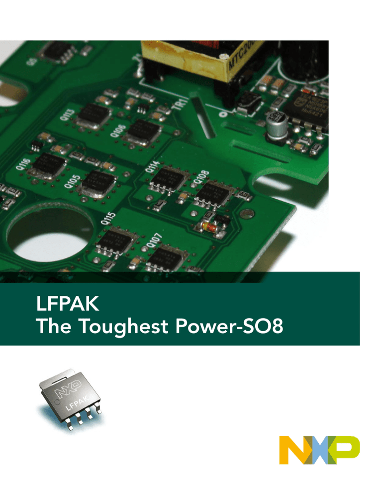
LFPAK
The Toughest Power-SO8
The evolution of Power MOSFET packages
Typical TO220 construction
TO220 is the ‘original’ through-hole power package. It is suitable for through-hole mounting and low-cost wave soldering.
It also provides very low thermal resistances when mounted to a suitable heatsink.
Benefits
}devices are ideal for through-hole PCB assembly & wave
soldering
}compatible with a wide variety of heat-sinking techniques
}low Rth(j-a) when mounted to a suitable heatsink
Limitations
} bond wires give significant package resistance, high
inductance, poor ID(max), and poor thermal performance
unless a heatsink is used
} physical size and weight
Typical D2PAK construction
D2PAK is a surface-mount variant of the TO220 package. The MOSFET is assembled in the same manner to TO220, but the DRAIN
tab and the GATE & SOURCE pins are modified to make the device suitable for surface mount and reflow soldering directly to a PCB.
Benefits
}Uses the PCB as a heatsink
}Compatible with pick & place machines and reflow soldering
}Lower package resistance & inductance than TO220 since
the DRAIN connection is made via the power-tab instead of
TO220 lead
Limitations
}Heat dissipation through the PCB may be limited compared
to a heatsink
}bond wires give high package resistance, high inductance &
poor ID(max) when compared to an LFPAK device
Typical DPAK construction
DPAK construction is similar to D2PAK, however the DPAK package outline is approximately 65mm2 compared to D2PAK 150mm2.
Benefits
} Uses the PCB as a heatsink
} Compatible with pick & place machines & reflow soldering
} Reduced PCB footprint when compared to D2PAK
Limitations
}Smaller silicon size means relatively high RDS(ON) values
}Fewer bond wires give high package resistance, high
inductance & poor ID(max) when compared to D2PAK
2
Loss Free PAcKage
The LFPAK package was developed as a ‘true’ power package; the package design has been optimised to give the best thermal &
electrical performance, cost and reliability.
Package resistance (mOhm)
LFPAK
D2PAK
TO220
DPAK
0
0.5
1
1.5
2
LFPAK construction
The silicon die is soldered to the DRAIN tab forming the electrical DRAIN connection and a low thermal resistance path to the PCB.
The top-clip is then soldered to the silicon die to provide SOURCE and GATE connections, eliminating the gold-wires and reducing
package resistance and inductance.
!
The DRAIN tab is soldered directly to the PCB to provide a low electrical resistance and also low thermal resistance between the
MOSFET and PCB.
Upper lead-frame bonded directly
to die giving reduced electrical
resistance & inductance in
source connection
LFPAK
Direct connection between
drain-tab-pcb results in
drastically reduced Rthj-mb
3
MOSFET assembly techniques
of competitor devices
3/#$%&'(
)*+,%+-#
!"#$%&'(
)*+,%+-#
!"#./%0#1##
3"#)"60#
Compare the LFPAK with competitor Power-SO8 types which are often constructed using wire or ribbon bonding as shown below.
LFPAK uses a combined copper clip which is soldered in a single operation to the GATE & SOURCE. This reduces the spreading
!
!
!
resistance, which is seen when bond wires are used and gives LFPAK superior electrical & thermal performance as well as increased
reliability when compared to many competitor Power-SO8 types.
Al wire-bonding
Cu wire-bonding
Cu clip & Au bump
89:3;#'
,'@%.'>#
89:3;#!
-%@'>E(##
• m
• l
• l
• s
Ribbon bond & wire GATE
Cu clip & wire GATE
Cu clip & wire GATE
LFPAK eliminates wire-bonding seen in
many competitor devices
LFPAK Combined GATE & SOURCE clip !
with soldered die-attach gives :
} maximum mechanical ruggedness
& reliability
} lowest electrical resistance
} lowest thermal resistance
} simplified manufacturing process
4
Tolerant to mechanical & thermal stress
Customer feedback consistently shows that LFPAK is more reliable & rugged than competitor 5x6mm QFN & micro-lead devices.
The following diagram shows that mechanical stress can occur when a device is rapidly heated or cooled causing cracking of the
MOSFET moulding and also solder joint failure under the GATE & SOURCE pins of a QFN device. LFPAK’s construction allows the
SOURCE & GATE pins to ‘flex’ and safely absorb any stress. Similar stresses on a QFN or micro-lead device often causes solder
joint failures and/or cracking of the plastic case which can lead to failures.
LFPAK is the only Power-SO8 device available with automotive qualification (AEC-Q101) which is clear proof of its superior
ruggedness & reliability under the toughest conditions.
Diagnosis & failure for QFN & micro-lead devices often requires costly X-ray analysis and specialist SMT rework equipment. LFPAK
solder joints can be visually inspected and it is possible to rework an LFPAK device using simple, low-cost rework tools.
Movement due to thermal and/or mechanical stress in PCB
Movement due to thermal and/or mechanical stress in PCB
Mechanical stresses occur when a SMT device is subject to rapid temperature change or if the PCB bends due to mechanical
strain or vibration.
The LFPAK’s exposed lead-frame provides compliance and allows for movement due to thermal expansion and mechanical strain.
QFN sawn & micro-lead packages are fully encapsulated and do not allow for movement due to thermal expansion or
mechanical strain. Mechanical & thermal stresses lead to solder-joint failures at the GATE & SOURCE pins.
Also cracking can occur in the mould material around the pins which can lead to moisture ingress & ionic contamination
causing degradation & early failure of the MOSFET.
5
LFPAK Thermal resistance
The thermal performance of a MOSFET when mounted to a PCB relies on two parameters.
Rth(j-mb) thermal resistance – junction to mounting base
For LFPAK and TO220 packages Rth(j-mb) is quoted on the datasheets and is typically 0.5 C/W to 2 C/W. This value depends on
the chip size for the silicon and generally increases as the silicon size decreases.
Rth(j-a) thermal resistance – mounting base to ambient
This value is quoted for TO220 devices and is not quoted for LFPAK devices – why is this?
For TO220 devices, Rth(j-a) represents the thermal resistance between the MOSFET junction and ambient (not connected to a
heatsink). Rth(j-a) represents a free-standing TO220 device and can be easily measured & characterised. Since it is possible to
mount & operate a TO220 device without a heatsink, then Rth(j-a) is useful for calculating the junction temperature and/or the
maximum allowable power dissipation for a free-standing TO220 device.
For LFPAK devices, the MOSFET’s DRAIN connection to the circuit relies on it being soldered to a PCB, it is not possible to operate
an LFPAK MOSFET in free-standing mode like a TO220 device. Therefore the thermal resistance Rth(j-a) for the MOSFET on its own
is not meaningful and cannot be measured. The thermal resistance should be approximated to the following expression (ignoring
any radiation & convection losses of the MOSFET).
Rth(j-a) = Rth(j-mb) + Rth(mb-a)
Since Rth(j-mb) is typically approx 1 C/W then the thermal performance is dominated by the thermal resistance of the PCB
Rth(mb-a) which varies widely and can be 40 - 100 times greater than the Rth(j-mb).
The graph shows Rth(j-a) for a 40 mm x 40 mm FR4 PCB. The simulation is for a simplified single LFPAK MOSFET mounted to a
copper footprint with dimensions length = width = x
The graph shows that the thermal performance is dependent on copper pad size and also the number and type of copper layers in
the PCB.
6
160.0
Layer 1 only
140.0
2-layer
4-layer
4-layer (layer 2 100% coverage)
120.0
4 layers - (4 x 5 vias)
Rthj-a (K/W)
100.0
80.0
60.0
40.0
20.0
10
15
20
25
30
Layer 1 side length "x" (mm)
Illustrates the PCB dimensions used for thermal
simulation
FR4 side length
40mm
FR4
"x"
LFPAK
MOSFET
Layer 1 copper of
side length "x"
Illustrates the use of thermal vias between layer-1 and layer-4, to
optimise the conduction of heat away from the LFPAK device.
Device
Layer 1 (power)
Layer 2, (ground)
Vias
Layer 3, (signal)
Layer 4, (power and signal)
7
LFPAK soldering & footprint compatibility
}There are many power MOSFETs available in the power-SO8 family. The following diagram shows that the package styles and
recommended PCB footprints differ significantly from each manufacturer. There is no generic JEDEC standard for Power-SO8
devices and therefore each device generally has a different PCB footprint as illustrated below.
}Fairchild
None of the manufacturers
guaranteed to be interchangeable
with
other
devices
Vishaydevices areInfineon
NEC
ON
Semi
STM
NXP
Power 56
PowerPak SO8
SuperSO8
HVSON-8
DFN6
PowerFlat 6x5
LFPAK
}LFPAK (SOT669 & SOT1023) achieves mechanical & electrical compatibility with the following Power-SO8 types. Each variant
may require a different solder-resist, solder-stencil and machine programming unless careful consideration has been made in
advance to design a universal footprint which will allow multiple devices to be fitted to the PCB
}The following diagram shows each manufacturers original footprint with their PowerSO8 mounted on it. The diagram below
shows the manufacturers footprint with an LFPAK mounted.
The diagram above shows that the LFPAK will provide basic electrical and mechanical compatibility with other manufacturers
Power-SO8 package footprint. Care must be taken to correctly specify the solder resist layer and solder stencil.
8
Through careful design of the PCB footprint , it is possible to design a universal footprint, such as the one shown below, that meets
the requirements of various PowerSO8 manufacturers. The example universal footprint shows the solder resist & solder stencil
details, which allow a PCB designer to create a footprint that is compatible with all of the following power-SO8 types.
4.7
4.2
0.25
(2¾)
0.9
(3¾)
0.25
(2¾)
0.6
(4¾)
3.45
0.6
(3¾)
3.5
2.55
2
0.25
(2¾)
SR opening =
Cu + 0.075
1.1
2.15
3.3
SP opening =
Cu 0.050
0.7
(4¾)
1.27
3.81
solder lands
solder paste
125 Mm stencil
solder resist
occupied area
sot669_fr
Recommended universal Power-SO8 & LFPAK footprint allows the following device types
to be mounted to a single PCB design:
}NXP LFPAK (SOT669 & SOT1023)
}Infineon PG-TDSON-8
}Fairchild Power 56
}Vishay PowerPAK SO-8
}NEC 8-pin HVSON
}ON Semi SO−8 FL
}STM PowerFLAT (6x5)
}Renesas LFPAK
The original document can be downloaded at : http://www.nxp.com/documents/reflow_soldering/sot669_fr.pdf
9
Notes
10
Notes
11
www.nxp.com
© 2009 NXP B.V.
All rights reserved. Reproduction in whole or in part is prohibited without the prior written
consent of the copyright owner. The information presented in this document does not
form part of any quotation or contract, is believed to be accurate and reliable and may be
changed without notice. No liability will be accepted by the publisher for any consequence
of its use. Publication thereof does not convey nor imply any license under patent- or other
industrial or intellectual property rights.
Date of release: December 2009
Document order number: 9397 750 16838
Printed in the Netherlands

