ADVANCE INFORMATION
PE826C32
Quad RS-422 Differential Line
Receiver
Product Description
The PE826C32 is a high performance monolithic CMOS
RS-422 line receiver. Its operating supply range is 3.0 to
3.6V, with an input signal common mode range of +/10V. The PE826C32 offers higher speed and lower
power than other RS-422 receiver types. It is packaged
in standard DIP and flat pack options and is ideal for
stringent military applications.
The PE826C32 is manufactured in Peregrine’s patented
Ultra Thin Silicon (UTSi®) CMOS process, offering the
performance of GaAs with the low power, economy and
integration of conventional CMOS.
Features
• High-speed operation: < 15 nS
typical
• Low power: < 9 mA typical
• 3.3 V operation
• Standard packaging: 16-lead
DIP and flat pack
• Pin Compatible with Existing
Industry Products
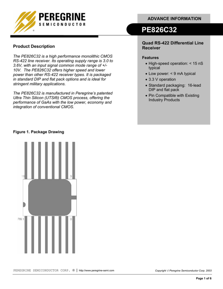
Figure 1. Package Drawing
PEREGRINE SEMICONDUCTOR CORP. |
http://www.peregrine-semi.com
Copyright Peregrine Semiconductor Corp. 2003
Page 1 of 6
PE826C32
Preliminary Specification
Figure 2. Pin Configuration
Table 2. Recommended Operating Conditions
Symbol
A-
1
16
V+
A+
2
15
D-
AQ
3
E+
14
4
BQ
5
B+
6
13
PE26C32
D+
DQ
12
E-
11
CQ
Parameter/Conditions
Min
Max
Units
V+
Supply voltage
3.0
3.6
V
TOP
Operating temperature
range
-55
125
°C
VIN (Line)
Maximum input voltage
A+/-, B+/-, C+/-, D+/-
-7
7
V
VIN (Dig)
Maximum input voltage
0
(V+)
V
Maximum output voltage
0
(V+)
V
IOUT
Maximum output current
-10
10
mA
VESD
ESD Voltage Human
Body Model (Note 1)
1000
V
VOUT
Note 1: Periodically sampled, not 100% tested. Tested per MIL-STD883 M3015 C2.
Electrostatic Discharge (ESD) Precautions
B-
7
10
C+
V-
8
9
C-
Table 1. Pin Descriptions
Pin
No.
Pin
Name
Latch-Up Avoidance
Description
1
A-
Channel A Inverting Input
2
A+
Channel A Noninverting Input
3
AQ
Channel A Output
4
E+
Enable, active high
5
BQ
Channel B Output
6
B+
Channel B Noninverting Input
7
B-
Channel B Inverting Input
8
V-
Ground Pin
9
C-
Channel C Inverting Input
10
C+
Channel C Noninverting Input
11
CQ
Channel C Ouput
12
E-
Enable, active low
13
DQ
Channel D Output
14
D+
Channel D Noninverting Input
15
D-
Channel D Inverting Input
16
V+
Supply Pin
Copyright Peregrine Semiconductor Corp. 2003
Page 2 of 6
When handling this UTSi device, observe the same
precautions that you would use with other ESDsensitive devices. Although this device contains
circuitry to protect it from damage due to ESD,
precautions should be taken to avoid exceeding the
rating specified in Table 2.
Unlike conventional CMOS devices, UTSi CMOS
devices are immune to latch-up.
Device Functional Considerations
The PE826C32 operates at high switching speeds.
In order to obtain maximum performance, it is
crucial that pin 16 be supplied with a bypass
capacitor to ground (pin 8).
Table 3. Truth Table
E+
E-
Vin (Diff)
Q
L
H
X
Z
H
X
<-200 mV
L
X
L
H
X
>+200 mV
H
X
L
H
X
Open
H
X
L
File No. 70/0146~00A
| UTSi CMOS RFIC SOLUTIONS
PE826C32
Advance Information
Table 4. Electrical Specifications
-55° C < Tcase < 125° C, 3.0 V < V+ < 3.6 V, PreRad, unless otherwise specified
Parameter
Minimum
Typical
Maximum
Units
3.0
3.3
3.6
V
5
10
mA
200
200
200
mV
mV
mV
100
mV
25 K
25 K
25 K
Ohms
Ohms
Ohms
1000
uA
(V+)*0.7
V
-1
1
uA
Input “Failsafe” Open Circuit Differential voltage
200
2500
mV
Output Drive Current @ 0.5 V from rail (high or low)
10
Output Short Circuit Current (to V-)
15
75
mA
Output Tristate Current, 0 < Vout < V+
-5
5
uA
Supply Voltage
Supply Current (Line inputs open, enabled)
(V+)=3.6V
Input Threshold (Line, differential)
VCM=+7
VCM=0
VCM=-7
-200
-200
-200
Input Threshold Hysteresis (Line, Differential)
VCM=0
5
Input Resistance (Line pins)
VCM=+7
VCM=0
VCM=-7
15
15 K
15 K
15 K
Input Current (Line pins)
VCM=+7
VCM=-7
-1200
Input Threshold (Enable)
(V+)*0.3
Input Current (Enable)
(V+)/2
mA
VOH @ 10 mA
(V+) – 0.5 V
(V+) – 0.4
(V+)
V
VOL @ 10 mA
0
0.4
0.5 V
V
TPHL (See Fig 2)
12
25
nS
TPLH (See Fig 2)
12
25
nS
TPZL, TPZH (See Fig 3)
10
25
nS
TPHZ, TPLZ (See Fig 3)
10
25
nS
50
FMAX
Notes:
MHz
(1) “Line” pins refer to A-, A+, B-, B+, C-, C+, D-, D+, differential outputs
(2) “Digital Input” or “Enable” pins refer to E+, E(3) “Digital Input” pins refer to AQ, BQ, CQ, DQ
(4) Output Short Circuit not intended to imply continuous operation
PEREGRINE SEMICONDUCTOR CORP. |
http://www.peregrine-semi.com
Copyright Peregrine Semiconductor Corp. 2003
Page 3 of 6
PE826C32
Preliminary Specification
Figure 3. TPLH, TPHL Test Circuit Block Diagram
TPLH, TPHL measured from input 50% to output
50% thresholds. TRISE, TFALL measured from
output 20% to output 80% thresholds.
4,16
DC
8,12
2,6,10,14
-
VI+
1.0 – 2.0
I-
3,5,11,13
+
1,7,9,15
I+
CL
15pF
VI1.0 – 2.0
Q
TPLH
TPLH
Figure 2: TPLH, TPHL
Q
TRISE
TFALL
Figure 4. TPLZ, TPZL, TPHZ, TPZH Test Circuit Block Diagram
TPZH, TPZL measured from input 50% to output
50% thresholds. TPHZ, TPLZ measured from
input 50% to output 10% thresholds.
16
DC
Vcc
3.3V
4
RL
2KΩ
2,6,10,14
+
13
E+/E0-(V+)
VI+ DC
L: 0.0
H: 1.5
1,7,9,15
DC
CL
15pF
E+
Q
VIL: 1.5
H: 0.0
Figure 3: TPHZ, TPZH, TPLZ, TPZL
Copyright Peregrine Semiconductor Corp. 2003
Page 4 of 6
3,5,11,13
E-
TPZH
TPHZ
TPZL
TPLZ
Q
File No. 70/0146~00A
| UTSi CMOS RFIC SOLUTIONS
PE826C32
Advance Information
Table 5. Ordering Information
Order
Code
Part Marking
Description
Shipping
Method
Package
826C32-01
PE826C32-01
Engineering Sample
16-pin DIP
1/Box
826C32-11
PE826C32-11
Production Unit, DIP
16-pin DIP
25/Tray
826C32-21
PE826C32-21
Production Unit, FP
16-lead FLAT PACK
25/Tray
826C32-00
PE826C32-EK
Evaluation Kit
Evaluation Board
1/Box
PEREGRINE SEMICONDUCTOR CORP. |
http://www.peregrine-semi.com
Copyright Peregrine Semiconductor Corp. 2003
Page 5 of 6
PE826C32
Preliminary Specification
Sales Offices
United States
Japan
Peregrine Semiconductor Corp.
Peregrine Semiconductor K.K.
6175 Nancy Ridge Drive
San Diego, CA 92121
Tel 1-858-455-0660
Fax 1-858-455-0770
5A-5, 5F Imperial Tower
1-1-1 Uchisaiwaicho, Chiyoda-ku
Tokyo 100-0011 Japan
Tel: 03-3507-5755
Fax: 03-3507-5601
Europe
Peregrine Semiconductor Europe
Aix-En-Provence Office
Parc Club du Golf, bat 9
13856 Aix-En-Provence Cedex 3
France
Tel 33-0-4-4239-3360
Fax 33-0-4-4239-7227
For a list of representatives in your area, please refer to our Web site at: http://www.peregrine-semi.com
Data Sheet Identification
Advance Information
The information in this data sheet is believed to be reliable. However,
The product is in a formative or design stage. The data sheet
contains design target specifications for product
development. Specifications and features may change in any
manner without notice.
Preliminary Specification
Peregrine assumes no liability for the use of this information. Use shall
be entirely at the user’s own risk.
No patent rights or licenses to any circuits described in this
data sheet are implied or granted to any third party.
Peregrine Space & Defense products are subject to export restrictions
The data sheet contains preliminary data. Additional data
may be added at a later date. Peregrine reserves the right to
change specifications at any time without notice in order to
supply the best possible product.
under both EAR (US Dept Of Commerce) and ITAR (USDept Of
State).
Contact Peregrine for current export restrictions, if any.
Peregrine’s products are not designed or intended for use in devices
or systems intended for surgical implant, or in other applications
Product Specification
intended to support or sustain life, or in any application in which the
The data sheet contains final data. In the event Peregrine
decides to change the specifications, Peregrine will notify
customers of the intended changes by issuing a PCN
(Product Change Notice).
personal injury or death might occur. Peregrine assumes no liability for
failure of the Peregrine product could create a situation in which
damages, including consequential or incidental damages, arising out
of the use of its products in such applications.
Peregrine products are protected under one or more of the following
U.S. patents: 6,090,648; 6,057,555; 5,973,382; 5,973,363; 5,930,638;
5,920,233; 5,895,957; 5,883,396; 5,864,162; 5,863,823; 5,861,336;
5,663,570; 5,610,790; 5,600,169; 5,596,205; 5,572,040; 5,492,857;
5,416,043. Other patents are pending.
Peregrine, SEL Safe, the Peregrine logotype, Peregrine Semiconductor Corp.
and UTSi are registered trademarks of Peregrine Semiconductor Corp.
Copyright © 2003 Peregrine Semiconductor Corp. All rights reserved.
Copyright Peregrine Semiconductor Corp. 2003
Page 6 of 6
File No. 70/0146~00A
| UTSi CMOS RFIC SOLUTIONS
