Extremely Thin
Profile Array Packages
A JCET Company
XFBGA, XFLGA, X1FLGA
HIGHLIGHTS
• Extremely thin packaging solutions
• Profile heights less than 0.50mm
• Advanced molding technology
• Extra thin design allows full array of solder
balls (BGA) or lands (LGA)
• Available in single or multiple die solutions
FEATURES
• Profile heights less than 0.50mm
• 0.25mm mold cap
• 50µm die thickness
• 0.11mm and 0.13mm substrate thickness (2 metal layer laminate substrate)
• Flexible body sizes ranging from 4 x 4mm to 15 x 15mm
• 0.80, 0.65 0.50 and 0.40mm ball pitch
• 50µm solder bumping on substrate
• Utilizes conventional wirebond equipment and processes
• Wide range of custom and open tool designs available
• Pb-free material set options (including low alpha materials)
• JEDEC standard compliant
APPLICATIONS
• Space constrained portable electronics such as cell phones, mini disk drives and miniaturized consumer electronics
• Memory cards and USB drives
• Stacked packages
DESCRIPTION
Space constrained portable electronics such as cell phones,
mini disk drives and miniaturized consumer electronics are driving the
need for smaller and thinner packaging solutions to support low vertical
profiles. By combining conventional wirebond equipment and processes
with advanced thinning technologies, STATS ChipPAC is able to offer
a leading edge solution that still satisfies the cost sensitive demands
of consumer applications: Extremely Thin Profile Array Packaging
solutions. STATS ChipPAC’s extremely thin packages offer maximum
profile heights less than 0.50mm.
While bare die solutions have typically been utilized for extremely
thin profile requirements, STATS ChipPAC offers the option of using a
substrate-based molded package for the same applications. These extra
thin packages are able to accommodate die shrinks without changing
the package footprint as well as integrate more than one device within
the package.
In order to achieve a maximum profile height less than 0.50 mm, STATS
ChipPAC utilizes a 0.11mm and 0.13mm two metal layer laminate
substrate, wafer thinning down to 50 microns, advanced molding
technology and an optimized bill of materials to minimize warpage of
the assembled package. STATS ChipPAC’s extra thin design allows a full array of solder balls or
lands on the substrate to deliver greater flexibility in input/output (I/O),
layout and density in a given package size. STATS ChipPAC’s Extremely
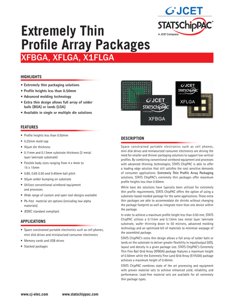
Thin Fine Ball Grid Array (XFBGA) package features a maximum height
of 0.50mm while the Extremely Fine Land Grid Array (X1FLGA) package
achieves a maximum height of 0.45mm.
STATS ChipPAC combines state of the art processing and equipment
with proven material sets to achieve enhanced yield, reliability, and
performance. Lead-free material sets are available for all extremely
thin package types.
www.cj-elec.com www.statschippac.com
Extremely Thin
Profile Array Packages
A JCET Company
XFBGA, XFLGA, X1FLGA
SPECIFICATIONS
RELIABILITY
Die Thickness
Mold Cap Thickness
Marking
Packing Options
Moisture Sensitivity Level
Temperature Cycling
50-100µm (2-4 mils)
0.25-0.30mm
Laser
Tape & Reel / JEDEC tray
JEDEC Level 2A, 260°C Reflow
Condition C (–65°C to 150°C),
1000 cycles
150°C, 1000 hrs
121°C/100% RH/2atm, 168 hrs
85°C/85% RH, 1000 hrs
130°C/85% RH/2 atm, 96 hrs
High Temp Storage
Pressure Cooker Test
Temperature/Humidity Test
Unbiased HAST
THERMAL PERFORMANCE, θja (°C/W)
Thermal performance is highly dependent on package size, die size, substrate layers and thickness, and solder ball configuration.
Simulation for specific applications should be performed to obtain maximum accuracy.
Package
XFBGA
Body Size (mm)
11 x 11 (2L)
Pin Count
144
Thermal Performance θja(ºC/W)
46.48
Die Size (mm)
4.5 x 4.5
Note: Simulation data for package mounted on 4 layer PCB (per JEDEC JESD51-9) under natural convection as defined in JESD51-2.
ELECTRICAL PERFORMANCE
Electrical parasitic data is highly dependent on the package layout. 3D electrical simulation can be used on the specific package design to provide the best
prediction of electrical behavior. First order approximations can be calculated using parasitics per unit length for the constituents of the signal path. Data below is for a frequency of 100MHz and assumes 1.0 mil gold bonding wire.
Conductor
Component
Wire Net (2L)
Total (2L)
Length
(mm)
2
2 - 7
Resistance
(mOhms)
120
25 -110
Inductance
(nH)
1.65
1.10 - 4.35
Inductance
Mutual (nH)
0.45 - 0.85
0.25 - 2.27
Capacitance
(pF)
0.10
0.20 - 0.90
Capacitance
Mutual (pF)
0.01 - 0.02
0.05 - 0.41
4 - 0
145 - 230
2.75 - 6.00
0.70 - 3.12
0.30 - 1.00
0.06 - 0.43
Note: Net = Total Trace Length + Via
CROSS-SECTION
PACKAGE CONFIGURATIONS
XFBGA
Body Sizes (mm)
4 x 4 to 15 x 15
Terminal Count
Terminal Pitch (mm)
8 to 200+
0.40 to 0.80
Typical Package Thickness
XFBGA: 0.50mm max.
XFLGA: 0.50mm max.
X1FLGA: 0.45mm max.
XFLGA
Corporate Office
Global Offices
10 Ang Mo Kio St. 65, #04-08/09 Techpoint, Singapore 569059 Tel: 65-6824-7777 Fax: 65-6720-7823
USA 510-979-8000
CHINA 86-21-5976-5858
KOREA 82-32-340-3114
SWITZERLAND 41-21-8047-200
The STATS ChipPAC logo is a registered trademark of STATS ChipPAC Pte. Ltd. Trademark registered in United States. Singapore company registration number 199407932D. All other product names and other company names herein are for identification purposes
only and may be the trademarks or registered trademarks of their respective owners. STATS ChipPAC disclaims any and all rights in those marks. STATS ChipPAC makes no guarantee or warranty of its accuracy in the information given, or that the use of such
information will not infringe on intellectual rights of third parties. Under no circumstances shall STATS ChipPAC be liable for any damages whatsoever arising out of the use of, or inability to use the materials in this document. STATS ChipPAC reserves the right
to change the information at any time and without notice.
©Copyright 2016. STATS ChipPAC Pte. Ltd. All rights reserved.
Apr 2016


