From schematic capture to PCB layout
advertisement

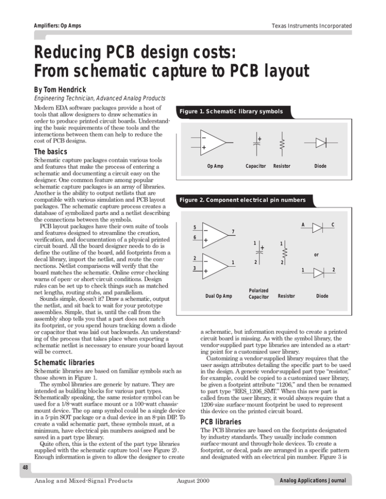
Amplifiers: Op Amps Texas Instruments Incorporated Reducing PCB design costs: From schematic capture to PCB layout By Tom Hendrick Engineering Technician, Advanced Analog Products Modern EDA software packages provide a host of tools that allow designers to draw schematics in order to produce printed circuit boards. Understanding the basic requirements of these tools and the interactions between them can help to reduce the cost of PCB designs. Figure 1. Schematic library symbols + The basics Schematic capture packages contain various tools Op Amp Resistor Diode Capacitor and features that make the process of entering a schematic and documenting a circuit easy on the designer. One common feature among popular schematic capture packages is an array of libraries. Another is the ability to output netlists that are compatible with various simulation and PCB layout Figure 2. Component electrical pin numbers packages. The schematic capture process creates a database of symbolized parts and a netlist describing the connections between the symbols. C A PCB layout packages have their own suite of tools 5 7 and features designed to streamline the creation, 6 verification, and documentation of a physical printed 1 1 circuit board. All the board designer needs to do is + define the outline of the board, add footprints from a or 2 decal library, import the netlist, and route the con2 2 1 nections. Netlist comparisons will verify that the 3 2 1 board matches the schematic. Online error checking warns of open- or short-circuit conditions. Design rules can be set up to check things such as matched Polarized net lengths, routing stubs, and parallelism. Dual Op Amp Diode Resistor Capacitor Sounds simple, doesn’t it? Draw a schematic, output the netlist, and sit back to wait for your prototype assemblies. Simple, that is, until the call from the assembly shop tells you that a part does not match its footprint, or you spend hours tracking down a diode a schematic, but information required to create a printed or capacitor that was laid out backwards. An understandcircuit board is missing. As with the symbol library, the ing of the process that takes place when exporting a vendor-supplied part type libraries are intended as a startschematic netlist is necessary to ensure your board layout ing point for a customized user library. will be correct. Customizing a vendor-supplied library requires that the Schematic libraries user assign attributes detailing the specific part to be used Schematic libraries are based on familiar symbols such as in the design. A generic vendor-supplied part type “resistor,” those shown in Figure 1. for example, could be copied to a customized user library, The symbol libraries are generic by nature. They are be given a footprint attribute “1206,” and then be renamed intended as building blocks for various part types. to part type “RES_1206_SMT.” When this new part is Schematically speaking, the same resistor symbol can be called from the user library, it would always require that a used for a 1/8-watt surface mount or a 100-watt chassis1206-size surface-mount footprint be used to represent mount device. The op amp symbol could be a single device this device on the printed circuit board. in a 5-pin SOT package or a dual device in an 8-pin DIP. To PCB libraries create a valid schematic part, these symbols must, at a The PCB libraries are based on the footprints designated minimum, have electrical pin numbers assigned and be by industry standards. They usually include common saved in a part type library. surface-mount and through-hole devices. To create a Quite often, this is the extent of the part type libraries footprint, or decal, pads are arranged in a specific pattern supplied with the schematic capture tool (see Figure 2). and designated with an electrical pin number. Figure 3 is Enough information is given to allow the designer to create 48 Analog and Mixed-Signal Products August 2000 Analog Applications Journal Amplifiers: Op Amps Texas Instruments Incorporated an example of some common footprints Figure 3. Example of common PCB footprints shipped with most PCB design tools. As with the schematic symbol library, one PCB decal can be associated with RES_. 25W 1206 many different part types. The layout database relies on the pin numbers defined in the schematic library for mapping to a footprint in the PCB library. This process allows two com8-SOIC 3216 pletely different 8-pin devices to use + 8-DIP the same 8-pin PCB decal. Understanding the importance of this SNAP_MT_CAP problem becomes even more obvious when you consider parts such as diodes or electrolytic capacitors. A generic schematic part called “DIODE,” for instance, could be assigned a PCB decal called “D0-41.” If Save time and avoid errors the diode is designated in the schematic library with elecAvoid using different platforms to produce schematic and trical pin 1 as the anode and electrical pin 2 as the cathode, PCB designs. Most EDA vendors can provide bundled the associated D0-41 footprint must also have the same schematic capture and PCB layout packages that are designations (see Figure 4). Having the pins reversed on designed to work together. These integrated packages the PCB footprint can cause serious problems that can be provide a common shell that allows for easier verification difficult to debug on an assembled board. Error checking of the schematic and board files, and makes processing will not catch this type of problem. engineering changes relatively painless. Integrated packages usually allow “back-annotation” as well, so that changes made in a PCB design can be reflected back to the schematic. Figure 4. Diode designation The use of a common library can help prevent problems. Develop a system where one regularly updated library serves the needs of all persons involved in design activities. Pin 1 Pin 2 Multiple people creating the same devices in individual 1 2 libraries will only lead to errors and confusion at layout. If a new part needs to be constructed, build it in a central library so everyone can use it. Review all newly created Diode Decal DO-41 parts and their associated PCB footprints for accuracy. Schematic Part Type PCB Decal PCB layout tools will normally present an error or warning if the schematic part references a PCB footprint with fewer electrical pins than described in the schematic netlist. For example, if a 14-pin device were assigned to an 8-pin decal, there would be an error mapping pins 9 The netlist file through 14 described in the schematic. If, on the other The netlist file is where the schematic and PCB databases hand, a 14-pin decal is assigned to an 8-pin device, error come together. The output from a schematic database is flags are not necessarily raised. A PCB decal can have formatted to meet the needs of a specific PCB layout more pins than electrically represented in a schematic; package and contains several specialized sections. mounting or alignment holes, for instance, are part of a The first section usually describes the PCB decals that decal. This type of error often goes unnoticed as well. It is are needed in the design. If a decal does not exist in the usually found after the PCB is fabricated, when someone PCB library, the desired part cannot be placed on the tries to mount a 14-pin device in a 16-pin decal. board. All schematic part types must be assigned a valid Many companies use outside sources to design printed PCB decal before the schematic netlist can be imported to circuit boards. If an external design house provides your the PCB design database. Most PCB design packages will printed circuit board layouts, make sure your engineers immediately flag an error and stop processing the netlist are familiar with the tools they use. Sending out a netlist file if a decal is missing. file in the correct format will save time and money. Share The next section of the netlist file contains the connecyour libraries with your vendor so they can save time and tion, or “rubber band,” information. If a decal cannot be avoid having to re-create parts. Create your schematic found, there can be no connections to route. Other sections libraries so that they reference the PCB footprint libraries may include PCB routing directives, simulation directives, of your design house. or detailed information for power and ground connections. 49 Analog Applications Journal August 2000 Analog and Mixed-Signal Products


