A Novel Technique for Driving Capability Improvement of a Class
advertisement
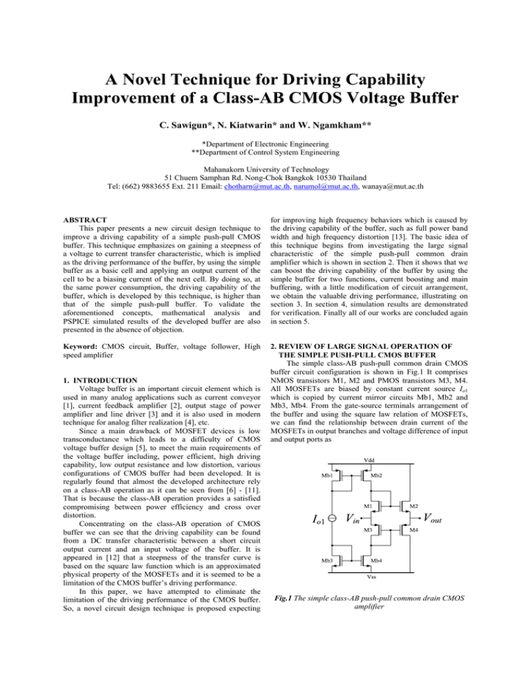
A Novel Technique for Driving Capability Improvement of a Class-AB CMOS Voltage Buffer C. Sawigun*, N. Kiatwarin* and W. Ngamkham** *Department of Electronic Engineering **Department of Control System Engineering Mahanakorn University of Technology 51 Chuem Samphan Rd. Nong-Chok Bangkok 10530 Thailand Tel: (662) 9883655 Ext. 211 Email: chotharn@mut.ac.th, narumol@mut.ac.th, wanaya@mut.ac.th ABSTRACT This paper presents a new circuit design technique to improve a driving capability of a simple push-pull CMOS buffer. This technique emphasizes on gaining a steepness of a voltage to current transfer characteristic, which is implied as the driving performance of the buffer, by using the simple buffer as a basic cell and applying an output current of the cell to be a biasing current of the next cell. By doing so, at the same power consumption, the driving capability of the buffer, which is developed by this technique, is higher than that of the simple push-pull buffer. To validate the aforementioned concepts, mathematical analysis and PSPICE simulated results of the developed buffer are also presented in the absence of objection. for improving high frequency behaviors which is caused by the driving capability of the buffer, such as full power band width and high frequency distortion [13]. The basic idea of this technique begins from investigating the large signal characteristic of the simple push-pull common drain amplifier which is shown in section 2. Then it shows that we can boost the driving capability of the buffer by using the simple buffer for two functions, current boosting and main buffering, with a little modification of circuit arrangement, we obtain the valuable driving performance, illustrating on section 3. In section 4, simulation results are demonstrated for verification. Finally all of our works are concluded again in section 5. Keyword: CMOS circuit, Buffer, voltage follower, High speed amplifier 2. REVIEW OF LARGE SIGNAL OPERATION OF THE SIMPLE PUSH-PULL CMOS BUFFER The simple class-AB push-pull common drain CMOS buffer circuit configuration is shown in Fig.1 It comprises NMOS transistors M1, M2 and PMOS transistors M3, M4. All MOSFETs are biased by constant current source Io1 which is copied by current mirror circuits Mb1, Mb2 and Mb3, Mb4. From the gate-source terminals arrangement of the buffer and using the square law relation of MOSFETs, we can find the relationship between drain current of the MOSFETs in output branches and voltage difference of input and output ports as 1. INTRODUCTION Voltage buffer is an important circuit element which is used in many analog applications such as current conveyor [1], current feedback amplifier [2], output stage of power amplifier and line driver [3] and it is also used in modern technique for analog filter realization [4], etc. Since a main drawback of MOSFET devices is low transconductance which leads to a difficulty of CMOS voltage buffer design [5], to meet the main requirements of the voltage buffer including, power efficient, high driving capability, low output resistance and low distortion, various configurations of CMOS buffer had been developed. It is regularly found that almost the developed architecture rely on a class-AB operation as it can be seen from [6] - [11]. That is because the class-AB operation provides a satisfied compromising between power efficiency and cross over distortion. Concentrating on the class-AB operation of CMOS buffer we can see that the driving capability can be found from a DC transfer characteristic between a short circuit output current and an input voltage of the buffer. It is appeared in [12] that a steepness of the transfer curve is based on the square law function which is an approximated physical property of the MOSFETs and it is seemed to be a limitation of the CMOS buffer’s driving performance. In this paper, we have attempted to eliminate the limitation of the driving performance of the CMOS buffer. So, a novel circuit design technique is proposed expecting Fig.1 The simple class-AB push-pull common drain CMOS amplifier 2 ⎛ = β 2 ⎜ (Vin − Vout ) + ⎜ ⎝ I o1 ⎞ ⎟ β1 ⎟⎠ ⎛ = β 4 ⎜ − (Vin − Vout ) + ⎜ ⎝ I o1 ⎞ ⎟ β 3 ⎟⎠ ID2 (1) and ID4 2 (2) W is a process transconductance L parameter of each MOSFET. After setting the process transconductance parameter β A = β1 = β 2 = β 3 = β 4 as a general symmetrical constraint, and considering a practical operation of MOSFETs, an output current of the buffer can be found to be Where β = 0.5k ' µ Cox ⎧ ⎪ ID2 ⎪ ⎪ ⎪ I out1 = ⎨ I D 4 ⎪ ⎪ ⎪ 4 (V − V ) β I in out A o1 ⎪⎩ if (Vin − Vout ) ≥ if (Vin − Vout ) ≤ − if − I o1 βA ≤ (Vin − Vout ) ≤ I o1 βA I o1 I o1 βA (3) From (3), it is clearly seen that the buffer is operated on class-A and B, depending on a voltage difference between input and output terminals (Vin-Vout = Vio). For small voltage difference signal − β A −1I o1 ≤ Vio ≤ β A −1I o1 the buffer is operated on class-A which is resulted from biasing in active mode for all MOSFETs. The voltage to current characteristics of the buffer in this range is a linear relationship. Therefore small signal output resistance of the buffer can be simply found to be rout1 = 1 4 β A I o1 Fig.2 The proposed buffer βA It can be observed that the current booster is biased by constant current source Io2 but the main buffer is biased by the output current of the first one. Drain currents of M2 and M4 are copied, by the current mirrors and supply to drain terminals of M5 and M7 as the biasing currents. From the last section, we have known that ID2 and ID4 are functions of Vio so a magnitude of an output current of this circuit which is increased by Vio at a higher rate will be achieved, illustrating in mathematical analysis below. Setting current transfer ratio of each current mirror to be unity, then we have I D6 (4) And if Vio is higher than this range, the output current of the buffer will be squarely increased as (1) until it is saturated. For the opposite direction, the buffer is vice versa operated, if Vio is less than that range the output current will be (2) until it is saturated, too. The driving performance of this circuit is identified by the square law function in (1) and (2) for positive and negative side of Vin, respectively. By means of improving the driving ability, the square law relations will be forced to be higher degree of increasing functions. In the next section, an improving method, based on the same basic operation of the simple buffer, to gain the driving performance will be presented. 3. THE PROPOSED TECHNIQUE In order to gain driving capability of the buffer, we have attempted to increase the steepness of the voltage to current transfer characteristic, especially in class-B region. To do so, the buffer in Fig.1 is used in the proposed buffer in Fig. 2, for two functions, the first one is used as the current boosting circuit M1-M4 and the other one M5-M8 is the main buffer, which are connected together by two current mirrors M9-M10 and M11-M12. ⎛ ⎛ ⎜ β 2 ⎜⎜ (Vin − Vout ) + ⎜ ⎝ = β 6 ⎜ (Vin − Vout ) + β5 ⎜ ⎜ ⎜ ⎝ 2 ⎞ I o1 ⎞ ⎟ ⎟ β1 ⎠⎟ ⎟ ⎟ ⎟ ⎟ ⎟ ⎠ 2 (5) and I D8 ⎛ ⎛ ⎜ β 4 ⎜⎜ − (Vin − Vout ) + ⎜ ⎝ = β8 ⎜ − (Vin − Vout ) + β7 ⎜ ⎜ ⎜ ⎝ 2 2 ⎞ I o1 ⎞ ⎟ ⎟ β 3 ⎟⎠ ⎟ ⎟ (6) ⎟ ⎟ ⎟ ⎠ For the sake of convenient and simplification, the buffers are supposed to be identical, resulting in β1 - β8 are equal with β B . For this reason, it can be approximated that ⎛ I I D 6 = β B ⎜ 2 (Vin − Vout ) + o1 ⎜ βB ⎝ ⎞ ⎟⎟ ⎠ 2 (7) and I D8 ⎛ I ⎞ = β B ⎜ −2 (Vin − Vout ) + o1 ⎟ ⎜ ⎟ β B ⎠ ⎝ 2 (8) Comparing the (7) and (8) with (1) and (2), we can see that the relationship between drain currents at output branches and the input voltage of the proposed buffer are, in parabolic form, similar to that of the simple one but the increasing rate is higher. In the similar way with section 2, we can summarize the output current of the proposed buffer as I out 2 ⎧ if (Vin − Vout ) ≥ ⎪ I D2 + I D6 ⎪ ⎪ I ⎪I + I − I if 0.5 o 2 ≤ (Vin − Vout ) < D6 D4 ⎪ D2 βB ⎪ ⎪ I = ⎨ I D 2 + I D 6 − ( I D 4 + I D 8 ) if − 0.5 o 2 < (Vin − Vout ) < 0.5 βB ⎪ ⎪ I ⎪I − ( I + I ) if − o 2 < (Vin − Vout ) ≤ −0.5 D4 D8 ⎪ D2 βB ⎪ ⎪ if (Vin − Vout ) ≤ − ⎪ I D 4 + I D8 ⎪⎩ Io2 βB Io2 βB Io2 βB Io2 βB Io2 βB (9) It is obvious that there are many regions occurred in circuit operation causing by different bias points in different stages of the buffer. Some regions are not significant for now, thus we can skip to the relevant regions. Consider operating point of the proposed buffer in the range of −0.5 β B−1I o 2 ≤ (Vin − Vout ) ≤ 0.5 β B−1I o 2 , we can show that I out 2 = 8Vio β B I o 2 + 4Vio β B I o 2 = 12Vio β B I o 2 (10) From (10), it is quite clear to see that voltage to current transfer characteristic of this range is linear and the small signal output resistance of the proposed buffer can be simply found to be 1 rout 2 = (11) 12 β B I o 2 In this range, all MOSFETs are biased in active region and the buffer is operated on class-A. Comparing (11) and (4) illustrates that the output resistance of the proposed buffer is three times smaller than the buffer in Fig.1. In fact, it is not fair to compare like this because power consumption and chip area are not included, in spite of the proposed buffer consumes more power and chip area which can be obviously seen from its circuit configuration. Trying to create a reasonable comparison we have neglected the biasing and current mirror circuits for simplification and we have set β A = 2 β B = 2 mA / V 2 and I o1 = 2 I o 2 = 2 µ A for equalizing transistor area and power consumption of the simple buffers in Fig.1 and the proposed buffer Fig.2. In the case of perfect matching CMOS devices, the theoretical relationship between push current (ID2 and ID6) and pull current (-ID4 and -ID8) of output branches of each buffer is plotted in Fig.3, demonstrating that an increasing rate of drain current in output branch of the proposed buffer (ID6 and ID8) is higher than that of the simple buffer in Fig.1. Thus, at this state, it can be claimed that the proposed buffer provide more transconductance and driving capability at the same power consumption. Fig.3 The push and pull current at output branches of the buffers in Figs.1 and 2 versus Vio at same power and die area consumptions 4. SIMULATION RESULTS To verify the theory in the last section the buffer in Fig.1 and Fig.2 have been simulated, by using 0.5 micron level 3 CMOS model parameter provided by [14] with PSPICE A/D in Orcad simulator, for two situations, DC sweep of short circuit current to demonstrate the maximum output current and transient response of the buffer while it was driving a paralleled 2 kΩ resistor and 50 pF capacitor load. Design parameters of both circuits are summarized in table 1 and the simulated results are shown in Fig.4 and Fig.5, respectively. Fig.4 illustrates a comparison between both buffer which shows that the proposed buffer provides larger maximum output current and small signal transconductance than that of the simple buffer. Fig.4 Comparative plotted of short circuit currents between the proposed buffer and the simple buffer out Fig.5 Transient response of the proposed buffer versus the simple buffer The transient response of both buffers is shown in Fig.5. It can be seen that the proposed buffer could drive load at higher speed and accuracy than that of the simple buffer. Including transistor area and power consumption, we have 180 (µm)2: 30 microwatt and 320 (µm)2: 25 microwatt approximately for the simple and proposed buffer, respectively. It can be seen that at a slightly difference of power consumption, the only one drawback of the proposed buffer is the larger area consuming. Table1: Design parameters The simple buffer in Fig 1. The proposed buffer Design parameters Mb1, Mb2 Mb3, Mb4 M1, M2 M3, M4 Io1 Mb5, Mb6, M9, M10 Mb7, Mb8, M11, M12 M1, M2, M5, M6 M3, M4, M7, M8 Io2 Values 30µm /1µm 10µm /1µm 20µm /1µm 60µm /1µm 2µA 30µm /1µm 10µm /1µm 10µm /1µm 30µm /1µm 1µA 5. CONCLUSION From the consistent results between the theory and simulation of the proposed technique using in CMOS buffer design shown in this paper. It can be ensured that, using the proposed technique, the driving capability of the class-AB push-pull CMOS buffer is successfully improved, leading to obtain higher speed and more power efficient suitable for being an output stage of low power voltage amplifiers. However, in the presence of the added current booster, we have to expense larger physical space and complexity in a circuit realization. Therefore, before using this buffer, it may need to be carefully considered to make a valuable decision in some applications. 6. REFERENCES [1] A. S. Sedra and K. C. Smith, “A Second Generation Current Conveyor and its Applications,” IEEE Trans Circuit Theory, vol. CT-17, pp. 132-134, 1970. [2] F. J. Lidgey and K. Hayatleh, “Current Feedback Operational Amplifiers and Applications,” Electronics & Communication Journal, pp. 178-182, Aug.1997. [3] N. P. Ramachandran, H. Dinc and A. I. Karsilayan, “A 3.3 V CMOS Adaptive Analog Video Line Driver With Low Distortion Performance,” IEEE J. Solid-State circuits, vol.38, no.6, pp. 1051-1058, Jun 2003. [4] K. Salama, “Continuous time universal filters using unity gain cells,” Int. J. Electron. Commun, no.2, pp. 1-4, 2002. [5] P. R. Gray, P. J. Hurst, S. H. Lewis and R. G. Meyer, Analysis and design of analog integrated circuits, 4th ed., John Wiley & Sons, Inc. USA, 2001, ch.5. [6] K. E. Brehmer and J.B. Wieser, “Large swing CMOS Power Amplifier,” IEEE J. Solid-State Circuits, vol. SC-18, pp. 624-629, Dec 1983. [7] J. A. Fischer, “A High-performance CMOS Power Amplifier,” IEEE J. Solid-State Circuits, vol. SC-20, pp.1200-1205, Dec 1985. [8] K. Manetakis and C. Toumazou, “A New HighFrequency Very Low Output-Impedance CMOS Buffer,” IEEE International Symposium on Circuits and Systems, 1996 [9] H. Elwan and M. Ismail, CMOS low noise class-AB Buffer,” Elec. Lett., vol. 35 no. 21, pp. 1834-1836, Oct 1999.. [10] You, F., Embabi, S. H. K. and Sinencio, E. S., “LowVoltage class-AB Buffers with Quiescent Current Control,” IEEE J. Solid-State circuits 33, pp. 915-919, Jun 1998. [11] Y. Ha, M. F. Li and A. Q. Liu, “A New CMOS Buffer Amplifier Design used in Low Voltage MEMS Interface Circuits,” Analog Integrated Circutis and Signal Processing 27, pp. 7-17, 2001. [12] K. Koli, CMOS Current Amplifier : Speed versus Nonlinearity, Ph.D. dissertation, Helsinki University of Technology, Finland, 2000. [13] E. M. Cherry, “Transient Intermodulation Distortion – Part I: Hard Non linearity,” IEEE Transaction on Acoustic, Speech and Signal processing, vol. ASSp-29, pp. 751-756, April 1981. [14] A. M. Ismail and A. M. Soliman, “Novel CMOS Current Feedback Op-Amp Realization suitable for High Frequency Applications,” IEEE Transaction on Circuit and Systems-I, vol.47, no.6, pp. 918-921, Jun 2000.

