TECH
BRIEF
The ESD Problem
What is ESD?
Electrostatic Discharge(ESD) is the transfer
of electrical charge between any two
objects. A common example of this is the
static shock that a person experiences after
walking across a carpet and then touching a
metallic object such as a door knob or file
cabinet. The “shock” is felt at the point of
contact and is typically accompanied by a
small spark and a slight snapping sound.
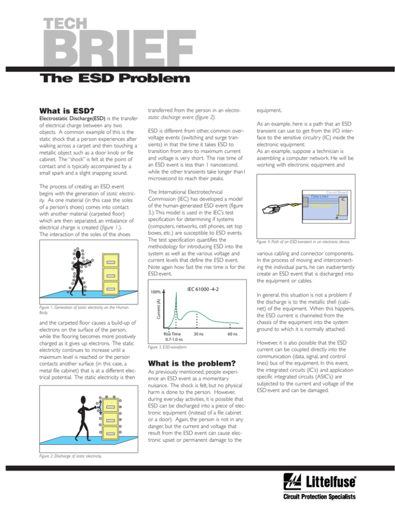
The process of creating an ESD event
begins with the generation of static electricity. As one material (in this case the soles
of a person’s shoes) comes into contact
with another material (carpeted floor)
which are then separated, an imbalance of
electrical charge is created (figure 1.).
The interaction of the soles of the shoes
transferred from the person in an electrostatic discharge event (figure 2).
ESD is different from other, common overvoltage events (switching and surge transients) in that the time it takes ESD to
transition from zero to maximum current
and voltage is very short. The rise time of
an ESD event is less than 1 nanosecond,
while the other transients take longer than1
microsecond to reach their peaks.
The International Electrotechnical
Commission (IEC) has developed a model
of the human-generated ESD event (figure
3.).This model is used in the IEC’s test
specification for determining if systems
(computers, networks, cell phones, set top
boxes, etc.) are susceptible to ESD events.
The test specification quantifies the
methodology for introducing ESD into the
system as well as the various voltage and
current levels that define the ESD event.
Note again how fast the rise time is for the
ESD event.
and the carpeted floor causes a build-up of
electrons on the surface of the person,
while the flooring becomes more positively
charged as it gives up electrons. The static
electricity continues to increase until a
maximum level is reached or the person
contacts another surface (in this case, a
metal file cabinet) that is at a different electrical potential. The static electricity is then
Figure 2. Discharge of static electricity.
As an example, here is a path that an ESD
transient can use to get from the I/O interface to the sensitive circuitry (IC) inside the
electronic equipment:
As an example, suppose a technician is
assembling a computer network. He will be
working with electronic equipment and
Circuit Board
Data Lines
IC
ESD Current
Figure 4. Path of an ESD transient in an electronic device.
various cabling and connector components.
In the process of moving and interconnecting the individual parts, he can inadvertently
create an ESD event that is discharged into
the equipment or cables.
IEC 61000 -4-2
100%
In general, this situation is not a problem if
the discharge is to the metallic shell (cabinet) of the equipment. When this happens,
the ESD current is channeled from the
chassis of the equipment into the system
ground to which it is normally attached.
Current (A)
Figure 1. Generation of static electricity on the Human
Body.
equipment.
Rise Time
0.7-1.0 ns
30 ns
60 ns
Figure 3. ESD waveform
What is the problem?
As previously mentioned, people experience an ESD event as a momentary
nuisance. The shock is felt, but no physical
harm is done to the person. However,
during everyday activities, it is possible that
ESD can be discharged into a piece of electronic equipment (instead of a file cabinet
or a door). Again, the person is not in any
danger, but the current and voltage that
result from the ESD event can cause electronic upset or permanent damage to the
However, it is also possible that the ESD
current can be coupled directly into the
communication (data, signal, and control
lines) bus of the equipment. In this event,
the integrated circuits (IC’s) and application
specific integrated circuits (ASIC’s) are
subjected to the current and voltage of the
ESD event and can be damaged.
What is the problem,
continued...
While these circuits have typical maximum
ESD protection levels of 2,000 V, humans
can generate ESD voltages in excess of
15,000 V. This level of ESD is in excess of
the on-chip protection circuits and can
damage them.
In the case of Junction Burnout, a short
circuit condition is created in a transistor of
the circuit.The metallic interconnect (trace
line) is “pulled through” one of the semiconductor layers (Alloy Spike) or one of
the semiconducting junctions is directly
short circuited (Junction Short).
Al
While the above example involved a technician assembling a computer network,
other examples include everyday users of
cell phones, computers, personal digital
assistants (PDA’s), set top boxes, and any
other electronic device.
Figure 6. Oxide Punch-Through
Once an ESD transient is discharged into
an electronic system, there are three
general types of adverse effects that the
ESD can generate in the electronic system:
In Oxide Punch-through, the metallic interconnect is “pulled through” the oxide layer
to provide a short circuit on the signal line.
Soft Failures
Data corruption can occur to a part of the
data stream, or the system may latch up.
This is a temporary problem and is solved
by data correction (for data corruption) or
by re-booting the system (for latch up).
Latent Defects
A component within the system may by
partially degraded, but is able to function
properly. A typical result of a latent defect
is that the system may experience premature failure due to the defective component.
SiO2
Oxide Short
Si
Dielectrics
Al
SiO2
Si
Interconnects
Figure 7. Metallization Burnout
In Metallization Burnout, the metallic interconnect is melted, much like a fuse. It
creates an open circuit condition on the
signal line.
What is the solution?
Catastrophic Failures
A component within the system is
rendered inoperable, and cannot function
properly.This is a permanent condition and
will not correct itself.This problem can
manifest itself as junction breakdowns, oxide
failures and the melting of interconnects.
This is the type of damage that is being
protected against by the use of ESD circuit
protection components.
Examples of catastrophic failures include:
Al
Junction
Short
E
Alloy Spike
B
C
Transistors
It should be reiterated that today’s IC’s and
ASIC’s include some level of on-chip
protection so that they can survive ESD
events that occur during chip and board
manufacturing processes. These are typified
in standards such as CDM (Charged Device
Model), MM (Machine Model), and HBM
(Human Body Model).
However, ESD transients seen by the end
product will be much more severe and
require off-chip, board-level ESD protection.
In future Technical Briefs, we’ll introduce the
solutions that are available to reduce catastrophic failures in electronic equipment
and allow the equipment to reliably withstand user-generated ESD events, as typified
in the IEC test specification 61000-4-2.
Littelfuse, Inc.
800 E. Northwest Highway
Des Plaines, IL 60016
(847) 824-1188
www.littelfuse.com/esd
Figure 5. Junction Burnout
Specifications, descriptions and illustrative material in this literature are as accurate as known at time of publication, but are
subject to change without notice. Littelfuse is a registered trademark of Littelfuse Incorporated.
EC621A
Copyright © 2001 Littelfuse, Inc., All Rights Reserved. Printed in U.S.A. JANUARY 2002


